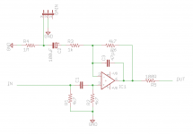
I've got some questions about this input stage that I was hoping someone could help me with 😀.
1) What is the purpose of R1? I'm used to only seeing R2
2) Isn't the value of R2 a bit low? Normally I see this around 100k
3) What is the purpose C2 and C3?
4) What would be a good value for C1? I'm thinking around 100uF given the value of R2?
5) If I wanted to add a RF low pass filter where should I put it and what values would be good?
Thank you 🙂

R1 stops the capacitor holding a charge before plugging in an input (stops the thump).
R2 is low, presumably to keep noise right down even without an input connected
C2 helps keep output DC offset low (DC gain is 1).
C3 is for stability - most opamps only need 0pF to 15pF here.
C1 is chosen for bandwidth - if you want 5Hz roll off then 6µ8 would work.
if you need an electrolytic then it should be sized much larger to prevent distortion, so 100µ might indeed be good choice.
Note the circuit is designed at low impedance, presumably to keep voltage noise down to a very low level - hence the 4k7 for R1/R2, and the 1k/4k7 feedback network. The gain jumper if shorted gives x5.7 gain, otherwise the circuit is a unity gain buffer.
The circuit is designed to be driven by a very low impedance source, again the assumption is low voltage noise.
Thank you so much Mark!
C1 at 6.8uF still leaves phase distortion up to around 100Hz right? (If my math is correct that is)
If I select the right op amp can I leave C3 out? It's only the older op amps that need it if I recall correctly?
Regarding source impedance, the op amp will see the combined impedance of the source itself plus up to 1/4 of an intervening potentiometer right? Assuming a 10k pot the op amp will see up to 2.5k plus source. The ratio of input to source impedance should be a minimum of 10:1 if memory serves. In this case R2 should be at least 25k I think?
Would higher values for the feedback network also be wise?
Last edited:
Depends what you call distortion - 1 degree? 0.01 degree? 4 degrees?Thank you so much Mark!
C1 at 6.8uF still leaves phase distortion up to around 100Hz right? (If my math is correct that is)
Not at all, its related to speed of opamp and whether its internally compensated for unity gain, nothing to do with age of design. If in doubt use a unity-gain stable opamp and a 22pF capacitor as well (close to the pins).If I select the right op amp can I leave C3 out? It's only the older op amps that need it if I recall correctly?
This circuit assumes a low impedance drive, not a volume pot. The input network will interact with the volume pot to distort its response. If you don't want low noise, all the impedances can be increased.Regarding source impedance, the op amp will see the combined impedance of the source itself plus up to 1/4 of an intervening potentiometer right? Assuming a 10k pot the op amp will see up to 2.5k plus source. The ratio of input to source impedance should be a minimum of 10:1 if memory serves. In this case R2 should be at least 25k I think?
As above, its a noise thing.Would higher values for the feedback network also be wise?
Note that the noise of the resistors (Johnson) plus the opamp input current noise multiplied by the source impedance on both input pins will contribute. A 10k source impedance generates 13nV/rtHz, and if the opamp has 1.6pA/rtHz current noise a further 16nV/rtHz will combine with that to give 21nV/rtHz (3µV rms for 20kHz bandwidth.
For line level this isn't a problem of course.
I've got some questions about this input stage that I was hoping someone could help me with 😀.
2) Isn't the value of R2 a bit low? Normally I see this around 100k
Thank you...
R2 looks chosen to match R6. This then cancels D.C. offset due to the op-amp's input bias currents by rendering the offsets as D.C. common-mode.
3) What is the purpose C2
As Mark said, C2 will turn the circuit into a unity gain follower at D.C., thereby minimizing the impact of any D.C. applied at the non-inverting input. However, this seems abit odd, as C2 will block any signal source D.C. anyhow. Perhaps, unwanted D.C. might be introduced via the jumper connected to R1.
Last edited:
As Mark said, C2 will turn the circuit into a unity gain follower at D.C., thereby minimizing it's impact if any were applied at the non-inverting input. However, this seems abit odd, as C2 will block any signal source D.C. anyhow. Perhaps, unwanted D.C. might be introduced via the jumper connected to R1.
Capacitor C2 prevents the circuit from amplifying the input offset voltage of the op amp.
The (maximum) signal gain is about 6x. Say the op amp spec is 1mV input offset.
Then without C2, the 1mV would be amplified to 1mV x 6 = 6mV DC at the output.
With C2, the gain at DC is x1, so the output voltage would be 1mV DC.
Last edited:
Thank you for all the information folks 🙂
Ah okay, that makes sense. Probably a good idea to increase R2 then if a pot is needed. That also means C1 can be a smaller value.
So would a value of 100k for R2 be okay for audio frequencies at line level?
I see something similar being used in the WHAMMY headphone amplifier (schematic here: WHAMMY headphone amplifier - diyAudio Guides )
As far as the AC signal is concerned, does the signal "see" R1 and R2 as being in parallel (i.e. a combined resistance of 2.35k)?
This circuit assumes a low impedance drive, not a volume pot. The input network will interact with the volume pot to distort its response.
Ah okay, that makes sense. Probably a good idea to increase R2 then if a pot is needed. That also means C1 can be a smaller value.
If you don't want low noise, all the impedances can be increased.
.
.
.
For line level this isn't a problem of course.
So would a value of 100k for R2 be okay for audio frequencies at line level?
However, this seems abit odd, as C2 will block any signal source D.C. anyhow. Perhaps, unwanted D.C. might be introduced via the jumper connected to R1.
I see something similar being used in the WHAMMY headphone amplifier (schematic here: WHAMMY headphone amplifier - diyAudio Guides )
As far as the AC signal is concerned, does the signal "see" R1 and R2 as being in parallel (i.e. a combined resistance of 2.35k)?
- Status
- Not open for further replies.
- Home
- Source & Line
- Analog Line Level
- Questions about this op amp input circuit