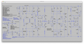
I've been experimenting with an all discrete BJT only DOA/buffer, for unity gain, or perhaps a gain of 2 or whatever.
Aiming for balanced inputs AND outputs, to drive a power amp with balanced inputs.
I made it work, but there is one issue that I've been wrestling with for a while that I haven't been able to solve:
It works but there is a HUGE offset that I can't get rid of.
I tried various ways to correct that offset, acting on the ltp negative input, both at the same time, acting on one of the inputs after the blocking cap, and even trying to act on the 2 tails, to force it back near zero. To no avail.
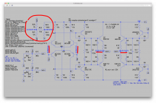
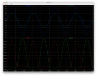
I'm attaching a screenshot of the simulation with my latest attempt.
The highlighted show how humongous the offset is. So much that it's much too close to the + rail and doesn't leave much headroom for the signal.
The signal comes out fine, as long as it's small enough.
My last attempt at forcing it to zero out, is that shenanigan circled red. which has a little effect but nowhere near enough, and causes more trouble that fixing it.
What could be done to make it properly balanced to have a low offset? Any ideas?
Aiming for balanced inputs AND outputs, to drive a power amp with balanced inputs.
I made it work, but there is one issue that I've been wrestling with for a while that I haven't been able to solve:
It works but there is a HUGE offset that I can't get rid of.
I tried various ways to correct that offset, acting on the ltp negative input, both at the same time, acting on one of the inputs after the blocking cap, and even trying to act on the 2 tails, to force it back near zero. To no avail.
I'm attaching a screenshot of the simulation with my latest attempt.
The highlighted show how humongous the offset is. So much that it's much too close to the + rail and doesn't leave much headroom for the signal.
The signal comes out fine, as long as it's small enough.
My last attempt at forcing it to zero out, is that shenanigan circled red. which has a little effect but nowhere near enough, and causes more trouble that fixing it.
What could be done to make it properly balanced to have a low offset? Any ideas?
Attachments
The gain doesn't change, the feedback is differential too, it needs no ground in the middle.Surely worth trying out.
Some kind of rudimentary servo.
But that'll change how the gain works. Let's see how this goes..
Mona
True! But there is one thing it will beat, it's not limited to 16V rails.
PLUS, although it's an amazingly high performing chip, it has one HUGE drawback for DIYers, at least for me, it's only SMT, and I wouldn't touch that with a 10ft pole.
This is all discrete, no SMT, all through hole stuff that's easy for DIYers to handle (like me).
And this discrete gizmo still has great performance capabilities anyway.
Ok, I tried that method with that additional transistor to force the offset down, but that only works dynamically to re-center the signal but without actually re-centering the bias.
So the actual huge dc offset is still there, even though with a signal it looks like it's operating about normally. With the signal centered, the bias isn't.
And this method would only act one way, bringing the offset down and away from the top rail. So if for some reason the parts had hfe the other way and the offset was in the other direction, then it wouldn't work in that case.
I tried with a somewhat small cap. That cap could be of higher value, for a longer time constant, but that wouldn't fix the issue of the bias when idling.
One other thing. I was able to bump up the signal and it was able to do it without that very early clipping, but looking at the inputs on the ltp, it's being overdriven. Probably due to that huge correction effect imposed by that little extra gizmo to force it to center.
And the thd is quite high.
If only one side is used, with unbalanced signal, then the thd @ 1k is less than 2ppm, so it can be a pretty good performing little dudad.
Attachments
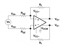
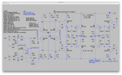
Taking that opa1632 as a reference, what I was trying to accomplish is somewhat similar, when not looking at the innards in that IC.
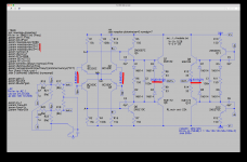
My "wiring" was basically the same as the typical usage, as on that first screenshot attachment.
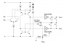
And that's when peeking at the IC's innards, that I can see they're definitely forcing the centering internally, with an error amp.
So, unless there is a simple way to make this work with little extra stuff, I suppose the only way will be to add on extra stage plus an error amp as well to make it work properly.
In any case, it's unlikely to beat that opa1632's stellar performance, but it can get fairly close and surely quite good enough to use, and most of all, it's 100% DIY stuff, that I would consider tackling. As I would never consider anything SMT for DIY...
My "wiring" was basically the same as the typical usage, as on that first screenshot attachment.
And that's when peeking at the IC's innards, that I can see they're definitely forcing the centering internally, with an error amp.
So, unless there is a simple way to make this work with little extra stuff, I suppose the only way will be to add on extra stage plus an error amp as well to make it work properly.
In any case, it's unlikely to beat that opa1632's stellar performance, but it can get fairly close and surely quite good enough to use, and most of all, it's 100% DIY stuff, that I would consider tackling. As I would never consider anything SMT for DIY...
Attachments
It can't function like that indeed, was a bit late last nightOk, I tried that method with that additional transistor to force the offset down, but that only works dynamically to re-center the signal but without actually re-centering the bias.
So the actual huge dc offset is still there, even though with a signal it looks like it's operating about normally. With the signal centered, the bias isn't.
And this method would only act one way, bringing the offset down and away from the top rail. So if for some reason the parts had hfe the other way and the offset was in the other direction, then it wouldn't work in that case.

The inputs has to be pulled negative, not to ground.
To other solutions i hope ?
First the same idea but to negative and another very simple without compensation.
Mona
Attachments
Worth trying. I'll try this out shortly.
But in the mean time, I've been pushing further the idea of adding an error correcting stage, and that required adding current sources and mirrors to the front end, but I think I got it right now, working properly and seems like great performance, possibly even beating that opa1632 beast in the process.
That is, in simulations of course. Real world might be a little less perfect and would definitely require matching parts (trans, res, caps...)
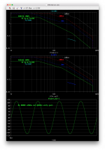
Ok, this isn't going to do it.
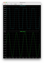
If we only look at what comes out on the real output, which is between out+ and out-, then it sort of looks like it works.
But when looking at it closer, it's really way off. The output from each side is totally clipped from its negative part of the cycles, and the full output only seems ok because each side's output is actually opposing in phase, so the resulting cycles look whole.
And the bias is definitely pulled down even closer to the V-. So basically the common mode offset is all the way down to V-, or very close to it.
I guess there won't be an easy way to do this, so my latest development is going to be the fully operational one. For which I'll post info in a moment...
Attachments
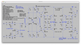
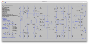
Here it is. More complex that my original plan, but this works pretty well now.
To be able to apply the corrections from that added diff error amp, I added current sources and mirrors to the front end, which isn't a bad thing, because it improved thd performance by more than one order of magnitude.
I geared it for unity gain and gave it an input to target about 3Vrms out.
So if this is correct, then it's beating the opa1632 performance.
There is a huge amount of headroom, with the rails at 28V, so this would almost never be pushed into clipping.
I loaded it with 2k, but it can handle lower load impedance pretty well.
Noise isn't too bad, with SNR close to 120db referred to ~3Vrms output.
Bandwidth pretty wide, with hardly any rolloff until well after 100khz, and I disabled the input dc blocking caps when I tried running it at 20hz and the caps add some thd. I made the input caps large, so they wouldn't affect thd much at low frequencies.
With them disabled, of course it passes dc.
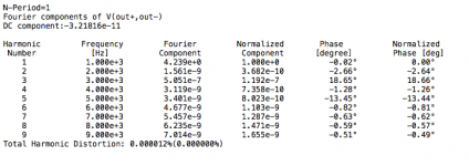
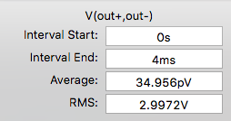
There is a small amount of common mode dc offset (less than 7mV), but the differential offset is quite tiny (DC component:-3.21816e-11), in the pV range.
Not a bad start. Maybe the compensation requires a bit of tweaking.
To be able to apply the corrections from that added diff error amp, I added current sources and mirrors to the front end, which isn't a bad thing, because it improved thd performance by more than one order of magnitude.
I geared it for unity gain and gave it an input to target about 3Vrms out.
So if this is correct, then it's beating the opa1632 performance.
There is a huge amount of headroom, with the rails at 28V, so this would almost never be pushed into clipping.
I loaded it with 2k, but it can handle lower load impedance pretty well.
Noise isn't too bad, with SNR close to 120db referred to ~3Vrms output.
Bandwidth pretty wide, with hardly any rolloff until well after 100khz, and I disabled the input dc blocking caps when I tried running it at 20hz and the caps add some thd. I made the input caps large, so they wouldn't affect thd much at low frequencies.
With them disabled, of course it passes dc.
There is a small amount of common mode dc offset (less than 7mV), but the differential offset is quite tiny (DC component:-3.21816e-11), in the pV range.
Not a bad start. Maybe the compensation requires a bit of tweaking.
Attachments
-
 Screen Shot 2019-05-20 at 3.49.58 PM.png530 KB · Views: 110
 -
 Screen Shot 2019-05-20 at 3.49.29 PM.png289.4 KB · Views: 109
 -
 Screen Shot 2019-05-20 at 3.50.10 PM.png55.7 KB · Views: 95
 -
 Screen Shot 2019-05-20 at 3.57.19 PM.png17.1 KB · Views: 22
 -
 Screen Shot 2019-05-20 at 3.58.56 PM.png234.1 KB · Views: 32
 -
 Screen Shot 2019-05-20 at 4.01.57 PM.png257.5 KB · Views: 30
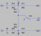
Filter/decoupling caps on the current source LEDs?
How is my hookup with the input resistances and feedbacks?
This needs to allow fully balanced XLR type of input and be used unbalanced without switching things.
With the gain bumped to 2 instead of unity, the performance is still good, somewhat the same, with a little higher thd.
How is my hookup with the input resistances and feedbacks?
This needs to allow fully balanced XLR type of input and be used unbalanced without switching things.
With the gain bumped to 2 instead of unity, the performance is still good, somewhat the same, with a little higher thd.
Common mode control of fully differential amplifiers is a well-known problem, and the solution is to use an ancillary feedback loop, dedicated solely to common-mode stabilization.
Fortunately, you found a solution by yourself, but you can find alternative ideas on the WWW and this site in particular, because the problem has surfaced a number of times, in power amplifiers or line amplifiers:
Fully differential and pseudo-differential stages
https://www.diyaudio.com/forums/sol...le-vas-current-amp-slone-book.html#post195526
Etc, etc
Thanks. Good stuff.
I had not double checked the output stage and vas bias again when I added the current mirrors, and it turns out the bias was a little too much on the "hot" side.
This is Class A, but there is far too much "reserve" there, and the vas trannies are pushed a little too hard for comfort, plus the outputs definitely require heatsinking.
So I'm tweaking things a little to lower the extreme dissipations. Losing a bit of thd performance in the process, but better make it safe.
Even with the low enough bias in the outputs, it would still be a good thing to heatsink them, just in case, for example if the load is down to 600ohms and the signal is pushed way beyond "normal" usage.
While doing some tweaking, I got the thd @20khz on 2k load down to .23ppm.
Not bad. And it went down to about .04ppm at some point @1khz on the same 2k load.
All this with 3Vrms output.
If I'm not mistaken, unless I interpret the datasheet info wrongly, those TO-92 types of trannies can dissipate 625mW @ Ta=25C.
This means, to me, that without doing anything to heatsink them, at ambient temps of no more than 25C, they ARE capable of dissipating those 625mW. They would certainly run hot, but withstand this harsh treatment.
Am I right?
I tweaked the vas biasing a little, and the vas trannies never dissipate peak power beyond about 420mW, regardless of load and the amp driven at 25Vpk on the output on a 600ohms load.
Adding a little heatsink to the vas trannies would keep them cooler, but even without that, they should handle it, isn't that right?
Now the outputs are almost always staying below their 1.5W max @ Ta=25C (no sink), and that's peak dissipation, not the average, which is far below that, and that's under the most extreme conditions of 600ohms load and pushed at 25Vpeak output.
Under any "normal" usage conditions, even pushed somewhat hard, it should handle the dissipation, but still, it's Class A and always dissipate quite a bit when idling.
So to be on the safe side, heatsinking is a must, for reliability's sake, long term.
Quite a few parts are dissipating a fair amount, due to that Class A biasing...
Thinking of the outputs emitter resistors, I was thinking some 1W ceramic types might be good to use, and they're non-inductive.
Something like this from mouser:
PCF1C330K KOA Speer | Mouser Europe
How about that? Good choice?
Something like this from mouser:
PCF1C330K KOA Speer | Mouser Europe
How about that? Good choice?
About the sim in entry 11, I don't understand.
With the voltages indicated Q13 is completely blocked, does nothing.The result is that the only difference with the original circuit is the juction R21-R22 isn't grounded directly but via R26.
And now the positieve voltages on in- and outputs become very negatieve ??
The max dissipation of TO-92 transistors with the collector in the middle is only allowed if the collector connection is less than 4mm from the circuit board and has a 1cm x 1cm copper surface at 25°C for cooling.
Mona
About the sim in entry 11, I don't understand.
With the voltages indicated Q13 is completely blocked, does nothing.The result is that the only difference with the original circuit is the juction R21-R22 isn't grounded directly but via R26.
And now the positieve voltages on in- and outputs become very negatieve ??
You're right. Now that you mention it, looking at those voltages there, it's no wonder it doesn't work.
I didn't have a 5V6 zener model, so I just went for that regular 4V7, but that's not what would make any difference.
Not only that tranny is blocked, it's even pretty well reversed biased.
Well, that was worth trying, but since that, I've made a lot of progress, and although it ended up much more complex that I planned at first, this is working mighty well now.
The max dissipation of TO-92 transistors with the collector in the middle is only allowed if the collector connection is less than 4mm from the circuit board and has a 1cm x 1cm copper surface at 25°C for cooling.
Mona
So they're counting on using the pcb as a heatsink then. Something to have in mind when laying out a pcb. But not matter, I think in any case it's better to just heatsink them all, as they will definitely run pretty warm from that Class A biasing.
Dissipation isn't an issue at all in all the rest, just the outputs and vas ones need some attention.
I've been tweaking and now the vas is biased at a bit less than 41mA, while the outputs are at a little over 46mA.
Peak dissipation in the vas trannies (TO-92) is at about 430mW (less than 350mW avg), and the outputs peak at about 1.28W (~1.22W), so they're pretty close to their max for no heatsinking and they really should be, even if only a small sink is used. Better than nothing, safe than sorry..
With unity gain and gain setting resistors at 5k, I'm looking at the common mode input impedance and differential input impedance, but it's a difficult compromise, because higher input impedance requires higher resistor values, which in turn greatly degrades the noise situation.
With low res values, the noise figures are very low, so basically the bulk of the noise is from those gain setting res.
And with that gain setup with the 5k res for unity gain, on a 2k load with a 3Vrms ouput, thd is "only" 1ppm @20khz. Drops to 0.06ppm @1khz, and just 0.03ppm @20hz. With the input dc blocking caps shorted of course, or the thd @20 will rise to 3.43ppm, with 1000u input caps.
The thd at the low freq rise a lot when the cap values drop. The bulk of the thd is then from the caps.
Here, I spent some time adding SOAs in plots, for the outputs for now. I'll add the ones for the vas trannies later.
I dropped the load to 600ohms and a unity gain, with about a +20dbu output (~7.75Vrms). Still far from clipping, but a fair amount of signal.
thd drops quite a bit with lighter load, lower level input and lower frequency of course.
At about 3Vrms output on a 2k load, still @20khz, thd drops to just 1ppm.
0.06ppm thd @1khz (same load and input)
0.03ppm thd @20hz
And with the input dc blocking caps always disabled, or thd is much higher with them on, even at the 1000u value...
Attachments

- Status
- This old topic is closed. If you want to reopen this topic, contact a moderator using the "Report Post" button.
- Home
- Source & Line
- Analog Line Level
- Buffer/DOA with balanced inputs/outputs