Hi there!
Im trying to build a input buffer for UCD250LP.
This is my first attempt to design a PCB, I need to get feedback.
Its based on the recommendations in the ucd 250lp datasheet.
Anyone care to take a look at it and see if I'm doing some really bad layout/design? Please 🙂
I guess there is a lot that can be done better. I know it looks like s**t compared to other pcbs I have seen.
I can share the KICAD files if anyone is interested.
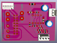
Schema:
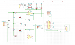
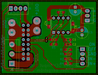
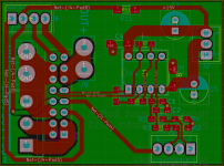
Top layer:
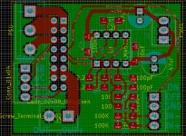
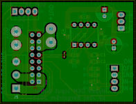
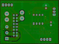
Bottom layer:
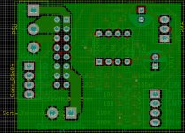
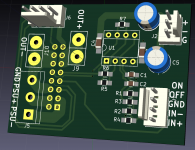
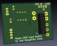
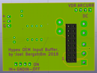
Pin assignment
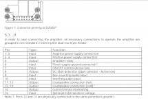
My plan is to do input buffers for the ucd400oem also.
Im trying to build a input buffer for UCD250LP.
This is my first attempt to design a PCB, I need to get feedback.
Its based on the recommendations in the ucd 250lp datasheet.
Anyone care to take a look at it and see if I'm doing some really bad layout/design? Please 🙂
I guess there is a lot that can be done better. I know it looks like s**t compared to other pcbs I have seen.
I can share the KICAD files if anyone is interested.
Schema:

Top layer:

Bottom layer:

Pin assignment

My plan is to do input buffers for the ucd400oem also.
Maybe I should specify some details.
This is for the Hypex UCD250LP oem module that sometimes can be bought from ebay and second hand. I bougt my 4 modules here at diyaudio (Swap meet). This pcb should work with the other hypex low profile modules as well I guess.
Some questions that comes to mind:
1. The op amp used is the LM4562NA DIP,
Is it better to use SMD version of lm4562 (any performance gains) or perhaps use any other op amp? OPA1612, OP2134?
2. Is 100nF + 47uF good values for the rails close to the LM 4562 in my design?
3. What kind of smd capacitors is good for this application, COG ?
4. Im going to hand solder the pcb. I have selected the 1206 size for all smd components, is it better (performance) to use smaller parts?
5. Is there ways to improve the layout regards to noise and performance?
Cheers!
Any thoughts at all? Would be great to know if I'm doing things wrong before ordering the pcbs. Its a long shipping time so I rather don't redo them if possible. Sure I will try to tidy some thing a bit before ordering.
I guess its a bit boring project because they are for oem amps that is not easily available, but I'm dong this for my private project, not commercial.
And Have just finished a pair of Lx521 open baffle speakers that needs a lot of amplifiers. So its kind of urgent 🙂 hehe.
I guess its a bit boring project because they are for oem amps that is not easily available, but I'm dong this for my private project, not commercial.
And Have just finished a pair of Lx521 open baffle speakers that needs a lot of amplifiers. So its kind of urgent 🙂 hehe.
Overall the design looks fine. I've made a few different UCD400 oem boards over the last year and in one I used the same basic buffer design as you're using and it works great.Any thoughts at all? Would be great to know if I'm doing things wrong before ordering the pcbs. Its a long shipping time so I rather don't redo them if possible. Sure I will try to tidy some thing a bit before ordering.
I guess its a bit boring project because they are for oem amps that is not easily available, but I'm dong this for my private project, not commercial.
And Have just finished a pair of Lx521 open baffle speakers that needs a lot of amplifiers. So its kind of urgent 🙂 hehe.
My only worry on your boards is if you've thought enough about how the UCD250LP will connect into the board, how the amplifier will then be heatsinked and with the amplifier connected are you going to be covering any of your other connectors. Those were issues I had and without knowing exactly what your plans are there might be a few "physical" things that could be better thought out. All in all looks pretty good for your first pcb.
Thanks for the response! The big connectors must be placed on the back of the board, away from the ucd. And the 18p connector and the rest of the components on the top side. Towards the ucd250lp. I will use a stright non angled connector to the ucd.
There might be a problem to keep the board in place only hold in place by the ucd connector.
There might be a problem to keep the board in place only hold in place by the ucd connector.
A couple of suggestions:
- Move C4 so it is parallel to R7 - then you can shorten the supply trace to the opamp.
- The routing on pins 1 + 2 on J6 could be shortened considerably if you route part of it in the ground plane layer (which shouldn't matter). You can exit the pin 2 trace on the correct side of J6 etc.
- If you swap R5 and R6 you don't have to route a trace under R6.
- I would think you can clean up the routing around R1-R4 (and the two caps) by experimenting with turning the components at right angles to each other. You want to go for shorter traces, not the best-looking component placement 🙂
- Etc.
And in general I think your traces look really thin, especially the ones than run through the connector pins. I would do what I could to get rid of those 🙂
Thanks for the feedback!
Since the buffer is differential/balanced I'd like to get the non-inverted and the inverted traces and components close to each other and in parallel as much as possible. I tried to look at how Bruno made his pre-amp input section.
But I guess It's room for improvement for sure. I'll try to put the components closer to each other for starters.
Picture from Brunos preamp: https://www.hypex.nl/img/upload/doc/an_wp/WP_The_G_word.pdf
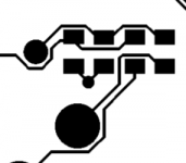
I'ts hard to route the traces to the dual pin header without going between the pins and still keep the traces close to each other. So the traces gets really thin.. I don't really know how to solve that one..
However. I'll be back with another version.
Since the buffer is differential/balanced I'd like to get the non-inverted and the inverted traces and components close to each other and in parallel as much as possible. I tried to look at how Bruno made his pre-amp input section.
But I guess It's room for improvement for sure. I'll try to put the components closer to each other for starters.
Picture from Brunos preamp: https://www.hypex.nl/img/upload/doc/an_wp/WP_The_G_word.pdf

I'ts hard to route the traces to the dual pin header without going between the pins and still keep the traces close to each other. So the traces gets really thin.. I don't really know how to solve that one..
However. I'll be back with another version.
Maybe I should specify some details.
This is for the Hypex UCD250LP oem module that sometimes can be bought from ebay and second hand. I bougt my 4 modules here at diyaudio (Swap meet). This pcb should work with the other hypex low profile modules as well I guess.
Some questions that comes to mind:
1. The op amp used is the LM4562NA DIP,
Is it better to use SMD version of lm4562 (any performance gains) or perhaps use any other op amp? OPA1612, OP2134?
2. Is 100nF + 47uF good values for the rails close to the LM 4562 in my design?
3. What kind of smd capacitors is good for this application, COG ?
4. Im going to hand solder the pcb. I have selected the 1206 size for all smd components, is it better (performance) to use smaller parts?
5. Is there ways to improve the layout regards to noise and performance?
Cheers!
LM4562 is about as good as it gets overall. Assuming you want 'wire with gain' and not 'colour'.
SMD device itself offers no advantage for the opamp itself - same just diffrent packaging. It does possibly allow a better layout - esp more continuous 0V 'plane' ; smaller loop areas - but it's marginal. DIP part allows use of socket.
Technically a socket distances the device from ground plane / decoupling etc and increases risk of connection failure. But really not an issue.
The big advantage is , of course, ease of switching op amps. If only to show how good yours is 🙂
Decoupling looks fine.
COG / NP0 ceramic caps - yes. Most stable and negligible voltage coefficient.
1206 components. No problem. Smaller components - I go down to 0603 - allow marginally tighter geometries.
But against that I think it's true (as in I've read it somewhere reputable - not measured it myself and not just someone saying it on an internet forum🙄 ) that larger resistors exhibit less noise - ie noise over and above the theoretical minimum noise.
On resistors - use Metal Film (MELF) / Thin Film types. Avoid Thick Film types. Linearity.
Thanks rmaudio!
Perhaps the boards are good enough by now, I will check them again for errors before ordering.
Any more suggestions of improvements are off course welcome!
Anyone want the cad files give me a PM.
Next step would be building a pcb for the Ucd400oem. (If no one are willing to share a design 🙂
However It should be quite easy to modify this board to use another pin-header to fit the Ucd400oem.
I have also thought about just replacing the op amp on the Ucd400oem with a LM4562 to improve the sound a bit. I'm not sure if Its a good idea thought. Hypex probably didn't design the decoupling the way they should have if they had chosen the lm4562 as the internal input buffer op amp from the beginning.
So I built the boards. Both for Ucd250 and Ucd400OEM. They turned out nice (can post pictures later) but I do have a problem with noise/hiss, especially coming from the Ucd250lp. They are fed with +-15V from a super regulator (ssr03). Its quite annoying, can't use them as long as thy is this noisy.
Any thoughts? Have I done a bad layout in some way?
Any thoughts? Have I done a bad layout in some way?
In my opinion connecting all the GND (inputs, power supply and outputs) on a ground plane is a bad thing and I think a ground loop is created.So I built the boards. Both for Ucd250 and Ucd400OEM. They turned out nice (can post pictures later) but I do have a problem with noise/hiss, especially coming from the Ucd250lp. They are fed with +-15V from a super regulator (ssr03). Its quite annoying, can't use them as long as thy is this noisy.
Any thoughts? Have I done a bad layout in some way?
Disagree. If your external wiring is correct then a single groundplane in an all-analogue circuit shouldn't create a problem**
**possible exceptions: mixed-mode analogue/digital boards and boards such as power amps with both high and low currents on the same board (here, everything is line-level)
**possible exceptions: mixed-mode analogue/digital boards and boards such as power amps with both high and low currents on the same board (here, everything is line-level)
In my opinion connecting all the GND (inputs, power supply and outputs) on a ground plane is a bad thing and I think a ground loop is created.
Does anybody have a photo or knowledge of hypex own input boards. How did they do it.
No, I do not have this.
One thing is certain is that I already did a preamplifier line with a ground plane where all the GNDs were connected and I had a big buzz, the problem was solved once the components disconnected from the ground plane and brought back to the mass well separately.
Maybe it's not normal or a coincidence but I already had this problem and now apart in the digital pcb all audio with a ground plan will gnd well separated.
Disagree. If your external wiring is correct then a single groundplane in an all-analogue circuit shouldn't create a problem**
**possible exceptions: mixed-mode analogue/digital boards and boards such as power amps with both high and low currents on the same board (here, everything is line-level)
I have the signal connected to rca, shield 100ohm/100nF to ground as described in the nc400 datasheet, possibly there could be improvements here, the wiring probably isn't optimal.
Attachments
Hi, did you found the problem? Are you building the amp with mains safety gnd connected to chassis?
I'm building 5 channel amp from UcD400OEM modules.
I'm planning to make custom input buffer boards as an upgrade later and would be interested (and wery grateful) if you have kicad files for those.
I'm building 5 channel amp from UcD400OEM modules.
I'm planning to make custom input buffer boards as an upgrade later and would be interested (and wery grateful) if you have kicad files for those.
Last edited:
JMSC you got a PM 🙂
Hi, did you found the problem? Are you building the amp with mains safety gnd connected to chassis?
I'm building 5 channel amp from UcD400OEM modules.
I'm planning to make custom input buffer boards as an upgrade later and would be interested (and wery grateful) if you have kicad files for those.
Hey Joel, nice work!
I'm also up to building a UCD400OEM amp, and I'd love to see your cad files ;-)
thanks a lot, regards
Enrico
I'm also up to building a UCD400OEM amp, and I'd love to see your cad files ;-)
thanks a lot, regards
Enrico
- Home
- Source & Line
- Analog Line Level
- Building UCD 250LP input buffer
