I'm trying to build a simple preamplifier that can be switched between passive, unity gain buffered and +6dB modes.
I am very new to all this, so could somebody with more experience have a look and tell me what can be improved? (And if it will even work?!)
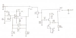
I've used an AD797 for the input, with RL1 selecting between unity gain and +6dB. This opamp stage can be bypassed altogether with RL2.
The output buffer is based on the the DC B1. This stage can also be bypassed RL3.
I have some specific questions:
1. I've calculated C1 & R1, and R2 & C2 to give -3dB at 1.59 Hz and 79.57 KHz respectively. Have I done this correctly? Do I need a resistor to ground before C1? How else can this area be improved?
2. I'm not sure about R5. The data sheet recommends 600 ohms, but obviously switching RL1 would cause this value to drop to 375 ohms. What 1K be better here?
3. Does the combined value of R3 and R4 have any significance (what's the difference between 3K and 1K vs 30K and 10K?)
4. My understanding is that the output buffer can be run without coupling caps (as with the DCB1), but since the opamp has gain, a DC blocking input cap is required. Is this correct?
Any help offered would be much appreciated!
I am very new to all this, so could somebody with more experience have a look and tell me what can be improved? (And if it will even work?!)
I've used an AD797 for the input, with RL1 selecting between unity gain and +6dB. This opamp stage can be bypassed altogether with RL2.
The output buffer is based on the the DC B1. This stage can also be bypassed RL3.
I have some specific questions:
1. I've calculated C1 & R1, and R2 & C2 to give -3dB at 1.59 Hz and 79.57 KHz respectively. Have I done this correctly? Do I need a resistor to ground before C1? How else can this area be improved?
2. I'm not sure about R5. The data sheet recommends 600 ohms, but obviously switching RL1 would cause this value to drop to 375 ohms. What 1K be better here?
3. Does the combined value of R3 and R4 have any significance (what's the difference between 3K and 1K vs 30K and 10K?)
4. My understanding is that the output buffer can be run without coupling caps (as with the DCB1), but since the opamp has gain, a DC blocking input cap is required. Is this correct?
Any help offered would be much appreciated!
Attachments
Why do you want to bypass the B1 output buffer, it only has a gain of ~1, the relay contacts only add an additional source of possible noise.
Unless you are lucky you could also end up with some "Woofer Busting" thumps when Relay 2 switches.
As you already have C1 at the input of the op-amp, I would consider a 10uF Polyprop (or better) at the output of the op-amp.
Unless you are lucky you could also end up with some "Woofer Busting" thumps when Relay 2 switches.
As you already have C1 at the input of the op-amp, I would consider a 10uF Polyprop (or better) at the output of the op-amp.
Last edited:
I'd like the bypass so I can easily compare the differences on the fly. For experimentation really. Bypassing the B1 isn't essential though.
Any way I could switch the opamp in and out of the circuit without any thumps?
Any way I could switch the opamp in and out of the circuit without any thumps?
2. I'm not sure about R5. The data sheet recommends 600 ohms, but obviously switching RL1 would cause this value to drop to 375 ohms. What 1K be better here?
3. Does the combined value of R3 and R4 have any significance (what's the difference between 3K and 1K vs 30K and 10K?)
4. My understanding is that the output buffer can be run without coupling caps (as with the DCB1), but since the opamp has gain, a DC blocking input cap is required. Is this correct?
Any help offered would be much appreciated!
It's been some while since I read the AD797 datasheet, but I strongly suspect that the 600 ohm output load is the recommended minimum. So, I suggest completely removing R5. I also suggest moving the contacts of RL-1 to be in series with R2 (the 1k resistor) to ground. This way, you automatically disconnect the 1K loading on the AD797 output when you switch to input buffering mode. In addition, I seem to recall that the AD797 doesn't like to have zero impedance betweeen it's output and inverting input, so this way would leave 3k of resistance between those two nodes - while 3k is not the best value for low noise, utilizing R3 reduces the amount of circuit alteration you would otherwise need perform.
Regarding the values of R3 and R4, while the ratio of the two determines the op-amp's closed-loop gain, their absolute values contribute to noise. The lower their absolute values the lower their (Johnson/Thermal noise). So, 3k and 1k resistors will have lower noise than 10k and 30k resistors. Resistor noise is often swamped by the noise of the active circuitry, (or even of the signal itself) however, the AD797 and the JFETs of the B1 stage are particulally low in noise. You might, quite logically, wonder why, say, 100 ohm and 300 ohm resistors aren't used for even lower noise. The problem, as you may have guessed, becomes the increasing distortion resulting from driving such a low impedance feedback network. It becomes a trade-off of noise versus distortion, having a number of system variables to consider.
Whether a B1 buffer stage can be run without an output capacitor depends on a couple of factors. I note that you have an input capacitor, so, that will take care of any D.C. offset on the input signal. The D.C. offset of the AD797 has nothing to do with gain, it is an parameter intrinsic to the device. The only real concern regarding D.C. offset which I see is the B1 stage. Although you arf utilizing bipolar supplies, the upper and lower half JFETs also have to very closely match. While you can well enough hand match those JFETs, I would be concerned about the different thermal conditions causing D.C. offset during operation. Best to use a good quality output cap., I suspect. 🙂
C1 should be 1uF for 1.59Hz . I would personally put in a 10uF non polarised electrolytic . Putting a resistor in front of C1 would only serve to reduce plug in clicks at the input......only relevant if you keep plugging and unplugging the input with the preamp on . C2 and R2 calc OK .
I would put a 47 Ohm resistor in series with the opamps output to ensure any possible capacitive loads on the output would not cause stability problems.
- Status
- Not open for further replies.