I generally prefer class-D amps, mostly for power efficiency, size and heat reasons. But I felt that, if for no other reason than "DIY Cred", I had to experience a Gainclone-style class-AB chipamp. Having low expectations, I went with the kit approach, and built a Neurochrome LM3886DR. I was pleasantly surprised at what I heard, and now feel compelled to wade a little deeper into the world of chipamps.
LM3886 has been done to death, and perhaps LM1875 has been too. But the 1875 is simpler. And furthermore, if this design is reasonable, maybe it can be a companion to the open-source lm3886 layout.
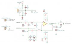
I started with the datasheet schematic (including using the same annotation), and made a few small tweaks:
PCB Notes:
Thanks for any feedback!
LM3886 has been done to death, and perhaps LM1875 has been too. But the 1875 is simpler. And furthermore, if this design is reasonable, maybe it can be a companion to the open-source lm3886 layout.
I started with the datasheet schematic (including using the same annotation), and made a few small tweaks:
- Input RF filter (R7, C8)
- Increased C2 to 220uF and added its protection diodes
- Completed Thiele network by adding L1 and R8
- Separate 0v reference from ground, connect with 10R resistor (or 0R at builder's discretion) at speaker return
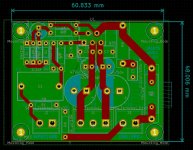
PCB Notes:
- The bottom copper layer is split. The left-hand 1/3 or so is the 0V reference ("small signal ground"), and the right-hand 2/3 is the power ground
- I intend to turn the +VDC, -VDC, 0v-to-GND, and speaker output traces into big copper pours. (Holding off on that until I get some feedback on the layout.)
- As with the open-source lm3886 layout, I intend to duplicate the 0v reference copper pour onto the top layer and stitch the two layers with vias
- Yes, the inductor will hang off the edge of the board
Thanks for any feedback!
Attachments
I suggest using pours (with appropriate thermal reliefs) for V+, V-, OUT, and the GND connection from the speaker GND to the signal GND through R6. Pours and wide traces have lower impedance (resistance and, less obvious, inductance) than skinny traces. You're paying for the copper anyway so you might as well use it.
You'd get slightly better performance if you take the feedback from R4/L1 as that compensates for the impedance of the output trace to that point. You may also find that you want the feedback ground (one end of C2) on the power ground rather than the signal ground as the feedback current can be pretty nasty. Just make sure you pick a quiet spot in the ground plane for this.
You might want to consider making C4 and C7 1.0 uF, X7R dielectric ceramic caps. You can see the impact of those here: LM3886 chip amp supply decoupling.
Nice work otherwise! You're ahead of most with this layout already.
Tom
This isn't related to layout, but what lead to the change in Thiele from the 5uH, 10R recommended in the datasheet?
Hi Tom, thank you for all the helpful feedback!
That is indeed the plan! It's somewhat time-consuming to create those pours, and it also makes the actual layout hard to read. I didn't want to run the risk of getting a bunch of negative feedback (pun intended) and have to entirely re-work the layout, and then have to redo all the pours.
Great, thanks again. I will study on that some more.
While I admit much of your "Taming the LM3886" series is a bit over my head, I nevertheless tried to get as much out of it as I can. (Clearly, most of the lm3886 best practices apply to the lm1875 as well.)
But a question: unless I'm missing something, it looks like you actually recommend 4.7uF, as opposed to 1.0uF? But your lm3886dr is using the latter...
The schematic is up for discussion as well!
I don't have a good technical reason for why those values were chosen. In fact, I forgot about the DS suggested values when I drew that up (since the DS doesn't show those components on their example schematic). But when I was doing my "homework", reading past lm1875 (and similar chipamp) threads, most people seemed to be using values closer to what I picked. Particularly with that inductor, the impression I got is the self-wound air cores of around 1uH are most common. Likewise, I see resistor values all over the map as well, anywhere from 2R to 10R.
What is the method to calculate optimal values for these components?
I suggest using pours (with appropriate thermal reliefs) for V+, V-, OUT, and the GND connection from the speaker GND to the signal GND through R6. Pours and wide traces have lower impedance (resistance and, less obvious, inductance) than skinny traces. You're paying for the copper anyway so you might as well use it.
That is indeed the plan! It's somewhat time-consuming to create those pours, and it also makes the actual layout hard to read. I didn't want to run the risk of getting a bunch of negative feedback (pun intended) and have to entirely re-work the layout, and then have to redo all the pours.
You'd get slightly better performance if you take the feedback from R4/L1 as that compensates for the impedance of the output trace to that point. You may also find that you want the feedback ground (one end of C2) on the power ground rather than the signal ground as the feedback current can be pretty nasty. Just make sure you pick a quiet spot in the ground plane for this.
Great, thanks again. I will study on that some more.
You might want to consider making C4 and C7 1.0 uF, X7R dielectric ceramic caps. You can see the impact of those here: LM3886 chip amp supply decoupling.
While I admit much of your "Taming the LM3886" series is a bit over my head, I nevertheless tried to get as much out of it as I can. (Clearly, most of the lm3886 best practices apply to the lm1875 as well.)
But a question: unless I'm missing something, it looks like you actually recommend 4.7uF, as opposed to 1.0uF? But your lm3886dr is using the latter...
This isn't related to layout, but what lead to the change in Thiele from the 5uH, 10R recommended in the datasheet?
The schematic is up for discussion as well!
I don't have a good technical reason for why those values were chosen. In fact, I forgot about the DS suggested values when I drew that up (since the DS doesn't show those components on their example schematic). But when I was doing my "homework", reading past lm1875 (and similar chipamp) threads, most people seemed to be using values closer to what I picked. Particularly with that inductor, the impression I got is the self-wound air cores of around 1uH are most common. Likewise, I see resistor values all over the map as well, anywhere from 2R to 10R.
What is the method to calculate optimal values for these components?
For once, I'm not quite sure it's the proper thing to do. Considering the included groundloop breaker resistor, you cannot return the feedback cap to the power ground without defeating its purpose. I posted a pair of sims on that in the other thread (mostly variations of your sims and Akitika's). That was pointed out to me by Mark Whitney (to give proper credit).You may also find that you want the feedback ground (one end of C2) on the power ground rather than the signal ground as the feedback current can be pretty nasty. Just make sure you pick a quiet spot in the ground plane for this.
Wrt the output inductor. I've finally found easier to solder the resistor under the board and solder the inductor on top. It's neater, more compact and alleviate the concerns of having a resistor inside an air core inductor. It's easier to do if you add a pair of holes for the inductor next to the holes for the resistor.
- Status
- Not open for further replies.