I'm getting ready to build up a VU meter with a pair of lm3916 for show, and also to monitor input to some amplifiers, and was curious as to which circuit from the datasheet would be a better general purpose use design, figure 5, figure 6, or figure 7.
I want peak hold, bar (not dot) style and average volume level to be read out. Would figure 5 or 6 be best for this? Any tips or ideas to make it better?
Also, would an lm324 quad opamp work for both channels, or should I use a basic pair of dual opamps like the opa2132p?
I want peak hold, bar (not dot) style and average volume level to be read out. Would figure 5 or 6 be best for this? Any tips or ideas to make it better?
Also, would an lm324 quad opamp work for both channels, or should I use a basic pair of dual opamps like the opa2132p?
I can't get Ti to locate the 3916 led driver. I only have the 3915 on my HDD.
Can you post a .pdf?
Can you post a .pdf?
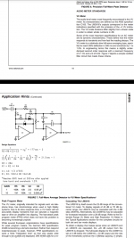
If you want a VU meter then use the VU meter style of circuit, i.e. fig7 into SIG.
If you want peak detecting, then feed Fig6 into the SIG.
Looks like you use pin9 for bar mode.
If you want peak detecting, then feed Fig6 into the SIG.
Looks like you use pin9 for bar mode.
If you want a VU meter then use the VU meter style of circuit, i.e. fig7 into SIG.
If you want peak detecting, then feed Fig6 into the SIG.
Looks like you use pin9 for bar mode.
Looks like figure 7 it is then.
Do you think building it up with a gain of 1, or gain of 10 would be more useful? I'm thinking 10 would be best, as it can simply be attenuated if needed.
Thanks!
more gain = more noise.
Do you want the bottom LED to be out when the signal is lower than the threshold for that LED?
Do you want the bottom LED to be out when the signal is lower than the threshold for that LED?
LM 3916 is desing to control recording level and other critical applications the scale have small dB steps around zero dB and the steps get bigger when you are far from 0 dB..
LM 3915 have 3dB steps all the way and is more usefull to monitor power level at the output of an amplifier ...
Unless you want to monitor to keep the amp just below clipping then go to LM 3916
LM 3914 is a linear scale but not a dB scale it is a voltage scale.
LM 3915 have 3dB steps all the way and is more usefull to monitor power level at the output of an amplifier ...
Unless you want to monitor to keep the amp just below clipping then go to LM 3916
LM 3914 is a linear scale but not a dB scale it is a voltage scale.
more gain = more noise.
Do you want the bottom LED to be out when the signal is lower than the threshold for that LED?
Yeah, I would like to have it out. I get what you are saying with regards to noise, I don't want unnecessary flickering of the LEDs.
LM 3916 is desing to control recording level and other critical applications the scale have small dB steps around zero dB and the steps get bigger when you are far from 0 dB..
LM 3915 have 3dB steps all the way and is more usefull to monitor power level at the output of an amplifier ...
Unless you want to monitor to keep the amp just below clipping then go to LM 3916
LM 3914 is a linear scale but not a dB scale it is a voltage scale.
Yup, per the thread title, I'm going to build the lm3916 up. The original question was which circuit from the datasheet would be best for the input circuitry.
I've attached the screenshot of the circuit, figure 7.
Attachments
Last edited:
- Status
- Not open for further replies.
- Home
- Source & Line
- Analog Line Level
- Which lm3916 circuit to build?