Hi
I consider replacing a 12 V switch mode PSU for my DAC with a linear PSU which is generally recommended. There are many custom made units on the market but I want to try a DIY project based on the LM317 or LM1086ADJ.
On the attached circuit (which I more or less as a principle want to follow) the electrolytic before the regulater is the largest (2200 uF) and the one at the output is only 100uF.
Other circuits show it opposite situation in the sense that the cap before the regulator is small and at the output is eg 6800uF.
Which solution is best from an audio point of view?
Thanks for helping
Torben
Attachments

The shown circuit is ample. Too much capacity on the output and the regulation won't work correctly. Ripple on the input doesn't matter as the regulator will not see it.
28Vac secondary may damage the 317 regulator during start up and/or if you set output to 1.2Vdc.
The two capacitors will each determine the ripple and that ripple depends on the current you draw and how fast you change that current.
The 2200uF first and 100uF last is normal.
The 0u33F is not normal. Remove it.
The two capacitors will each determine the ripple and that ripple depends on the current you draw and how fast you change that current.
The 2200uF first and 100uF last is normal.
The 0u33F is not normal. Remove it.
Last edited:
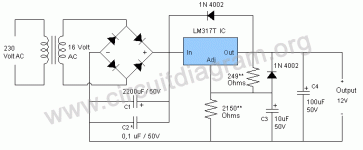
Thank you for commenting on the circuit. I have changed the drawing to show the exact values that will be implemented to fix the output voltage at 12 V which is the value that my DAC needs.
* C2 is supposed to be a 0,1 uF ceramic and should only be necessary if C1 is far from the LM317.
** the resistors are E96/1% metal film.
I understand that C4 must be a smaller capacity than C1 if the PSU is going to behave well without possible risks of malfunction.
Now for the core question: Many commercial PSUs made to replace switch mode PSUs for DACs boast huge values of capacity to be able to satisfy the need for
current. Is it then at the C1 position that the large capacitor bank is situated?
BR
Torben
Attachments
It is conceivable that the huge capacitance is intended to satisfy the need for marketing.klitgt said:Many commercial PSUs made to replace switch mode PSUs for DACs boast huge values of capacity to be able to satisfy the need for current.
In any case, putting a huge capacitance at the output of a regulator rather misses the point of a regulator and may affect its feedback loop stability. If you really need a huge capacitance then maybe you need a low value resistor between the regulator and the cap to ensure that only the cap sees the audio, and the regulator doesn't see the cap.
Last edited:
then move C2 to beside the 317. At the IN pin and the bottom end of the adjust resistor string...............* C2 is supposed to be a 0,1 uF ceramic and should only be necessary if C1 is far from the LM317..............
Not beside the smoothing capacitor.
circuit shown in post #4 is correct. DF96 is correct too.
In operation you should monitor the output voltage with an O-scope, if any unusual current demands that the V regulator and 100uF output cap is unable to cope with should be visible. I see both Vadj pin and Vout has protection diodes present for caps there.
otherwise (very unlikely for DAC chips ) some extra bypass caps should be placed closer to the load to help those short term current demands. National (TI) and LinearTech have very good app notes discussing all of these subjects.
Basically Vin > Vout +3V under all conditions of line and load.
the higher Vin is, puts more thermal loading on 3 terminal devices. So selection of transformer and largest cap (Vripple) is key
Last edited:
Many commercial PSUs made to replace switch mode PSUs for DACs boast huge values of capacity to be able to satisfy the need for
current. Is it then at the C1 position that the large capacitor bank is situated?
point them out please,
probably just puffery to market them against industrial products.
point them out please,
probably just puffery to market them against industrial products.
Sorry, I did not bookmark all the sites where I have read about the importance of large capacitor values. I can remember one provider who claims the importance of low impedance and high ripple current capacitors which I believe makes sense?
Squeeze-upgrade | High-end lineaire voeding met SBooster upgrade - Squeeze-upgrade | Sbooster | Audiophile power supply upgrades
AND there are general truths that no one denies, BUT it's all in the details!
... if something is good doesn't mean massive quantities of it are necessarily for the better.
that's what makes good Engineering, its a balance of all the factors.
... if something is good doesn't mean massive quantities of it are necessarily for the better.
that's what makes good Engineering, its a balance of all the factors.
Note that +5v drop gives the lowest noise, more than this is wasting power and generating heat. There is a reason the tests in the datasheet mention +5v drop in to out 😉
Tony.
Tony.
I posted above in a hurry on the train. The other thing I was going to say is that the main thing you need to worry about with the output cap is ESR. Too low and the cap will form a resonant circuit with the inherent output impedance of the regulator.
Bigger caps present two problems in this regard, the first is that they inherently have lower ESR, and the second is that the bigger the cap the lower the resonant frequency. If you use a large cap (say 1000uF) the resonant frequency will more than likely be smack bang in the middle of the audible frequency range!
You can deal with this by inserting some resistance between zero volts and the cap, which will damp the resonance.
I'm not going to get into anything about big caps slowing the reg down (affecting it's ability to react to the changes) as I have not done enough research or experimentation on this to venture an opinion. What I will say is that I do use a 1000uF cap on the output of my LM317 circuit with 0.3 ohms series resistance, and have not had any problems with it).
The comments above are based on my research and own experimentation. I am not an EE 😀
Tony.
I've always seen +3V for the old National data sheets, but +5V is realistically what you end up with accounting for line variation, input ripple and small EI transformer regulation under worst case loading. The newer devices all have been stretching for lower drop outs im sure.There is a reason the tests in the datasheet mention +5v drop in to out.
the noise specs are derived the band-gap reference and there-in lies the secret sauce , each semi house uses their own reference designs , so not all LM317 are created equal>
most don't have any guarantees on noise anyhoo
Last edited:
+3V is the dropout voltage from memory, but as far as I can remember, all the datasheets when presenting the noise stats state that the measurements were taken with 5V in - out differential 🙂
I basically did experiments with LT317A's and found progressive reduction in noise from 3V to 5V in-out differential, once I hit 5V there was no further improvement.
Tony.
I basically did experiments with LT317A's and found progressive reduction in noise from 3V to 5V in-out differential, once I hit 5V there was no further improvement.
Tony.
Hi Tony
good to know that about LinearTech re +5V , AFAIK they are the only vendor that offers an improved noise LM317.
was that on your PCB , did you happen to notice if the pnp on the adjust pin changed things?
good to know that about LinearTech re +5V , AFAIK they are the only vendor that offers an improved noise LM317.
I basically did experiments with LT317A's and found progressive reduction in noise from 3V to 5V in-out differential, once I hit 5V there was no further improvement
was that on your PCB , did you happen to notice if the pnp on the adjust pin changed things?
Last edited:
That's a good question! I did do testing with both standard circuit and with the transistor, from memory the transistor definitely improved the noise. I do not remember if I did the voltage experiment (ie increasing voltage before reg) with just the standard circuit.
OK here is a post with comparison between with and without the bc560C http://www.diyaudio.com/forums/power-supplies/188975-lm317-experiments-measurements.html#post2573524
Note that these were done on the breadboard implementation not the final verro board one.
Tony.
OK here is a post with comparison between with and without the bc560C http://www.diyaudio.com/forums/power-supplies/188975-lm317-experiments-measurements.html#post2573524
Note that these were done on the breadboard implementation not the final verro board one.
Tony.
I had a look back through that thread, and the one place I posted about different voltage (4V - 5V differential) looks very suspect, and I was dropping the ouput voltage, NOT increasing the input voltage (I thought I'd done the test using a variable voltage source).. So perhaps my comment should be taken with a grain of salt!
Tony.
Tony.
I looked at the LT specs and yer are right about the 5V headroom.
also interesting they list typical noise 3 times less than the generic STM part. But no one lists a maximum value.
might be a testing BW thing
the LT317 is the same part just laser trimmed reference> for fixed voltage apps.
off hand I think yer pnp junction throws off the temp stability. just looking at the lead acid battery charger diagram they show.
Possible about the temp, I hadn't really thought about it... I had made a comment about testing with different Hfe transistors without allowing for warm up.. It seems pretty stable though. It's been on for a few months now (I don't turn it off it draws so little power) I could measure voltage, turn it off for a few hours and then measure at startup and see if there is any difference 🙂
Tony.
Tony.
- Status
- Not open for further replies.
- Home
- Amplifiers
- Power Supplies
- Where to put the largest capacitor?