Can someone explain why a class d amp needs dead time?
From my understanding (which i guess must be wrong), i can see no need for it. The principle of PWM means that the width of the pulses is modulated to represent the signal. Small signal levels make short pulses, large signal levels make long pulses. Short pulses have long gaps between them, large pulses have small gaps. Small signal levels near the zero crossing of the input waveform, when the output devices are about to switch from one side to the other, hence the need for dead time to avoid turning on together) would be represented by very short pulses, and with short pulses there are large gaps between pulses. If there are large gaps between short pulses, why does there need to be additional dead time since the output would only switch between high side and low side when crossing the zero level, when the signals levels would be low, and the pulses short and with large gaps.
Evidently i am missing something here - i must have misunderstood some aspect of how this thing works. Any help much appreciated.
The dead time that's needed is the dead time you mentioned here:
.... the output devices are about to switch from one side to the other, hence the need for dead time to avoid turning on together)...
Dead time is to prevent shoot-through between output devices.
.... the output devices are about to switch from one side to the other, hence the need for dead time to avoid turning on together)...
Dead time is to prevent shoot-through between output devices.
Prevents smoke. It takes a finite time to turn on or off a device, especially mosfets, as their gates are effectively capacitors, and it takes time to charge/discharge a capacitor.
Dead time allows for the charge/discharge times.
If you ignored it, both devices would be on at the same time, allowing a short circuit between power and earth, or +vs to -vs.
EI. smoke.
LOTS of smoke.
Dead time allows for the charge/discharge times.
If you ignored it, both devices would be on at the same time, allowing a short circuit between power and earth, or +vs to -vs.
EI. smoke.
LOTS of smoke.
As i mentioned in my post, when the signal is about to crossover from one rail to the other, the pulse width is so short because of the low level of the signal that there already is a very large gap between pulses - why does there need to be more? To produce pulses of varying widths, the output devices must be able to switch on and off quickly enough to leave gaps between the pulses. Why is leaving a gap between pulses more difficult when moving from one device to another, as opposed to on the same device? Surely it should be easier.
Sorry but still do not understand.
Sorry but still do not understand.
I think you may be confused about the representation of small signals. The output stage is not tri-state; it only has two states. One state with low side on and high side off, the other state has high on and low off.
A zero level input turns into a 50% duty cycle at the output. Ideally, there is no signal-related moment when both devices are off. The amplifier always has one or the other switch on, or is transitioning from one switch to the other. Very low and very high duty cycles represent large signals near the power supply rail, ie near clipping.
To understand the need for dead time, forget about the signal and just think about what happens when you simultaneously turn off the low side switch and turn on the high side switch. Both switches take finite time to turn on or off. So there will be some ns or 10s of ns when both switches are partially on, forming a very small resistor between the power rails. Ouch, that damn thing it HOT and it smells funny if you get what I'm saying.
So we intentionally add some time to let the first switch turn off completely before the second switch turns on.
"The output stage is not tri-state"
Tri-State = Dead time!
During this time, the voltage at the inductor can not be controlled, so this means adding an output-current-dependant uncontrolled component to the Volt-Seconds-Product given to the inductor every cycle. The higher the dead-time, the higher the resulting distortion, so we want to avoid dead-time as far as possible, less than 50ns per cycle.
oh i see - perhaps
You are quite right about me being confused, perhaps more than ever!
Are you saying that the on state is with the high side on and the other off, and the off state is with the low side on and the high side off?
I thought that one switch handled handled half the wave form, and the other switch the other half. So that when the top half of the signal was being output, that only one switch was pulsing, then the other switch would take over for the second half of the waveform. This is not so?
Why not simply have a single switch and single supply rail (with twice the voltage), and do away with all the problems with dead time and the accompanying distortion?
🙄
I think you may be confused about the representation of small signals. The output stage is not tri-state; it only has two states. One state with low side on and high side off, the other state has high on and low off.
A zero level input turns into a 50% duty cycle at the output. Ideally, there is no signal-related moment when both devices are off. The amplifier always has one or the other switch on, or is transitioning from one switch to the other. Very low and very high duty cycles represent large signals near the power supply rail, ie near clipping.
To understand the need for dead time, forget about the signal and just think about what happens when you simultaneously turn off the low side switch and turn on the high side switch. Both switches take finite time to turn on or off. So there will be some ns or 10s of ns when both switches are partially on, forming a very small resistor between the power rails. Ouch, that damn thing it HOT and it smells funny if you get what I'm saying.
So we intentionally add some time to let the first switch turn off completely before the second switch turns on.
You are quite right about me being confused, perhaps more than ever!
Are you saying that the on state is with the high side on and the other off, and the off state is with the low side on and the high side off?
I thought that one switch handled handled half the wave form, and the other switch the other half. So that when the top half of the signal was being output, that only one switch was pulsing, then the other switch would take over for the second half of the waveform. This is not so?
Why not simply have a single switch and single supply rail (with twice the voltage), and do away with all the problems with dead time and the accompanying distortion?
🙄
If you have only a single switch (say to the -ve rail) then where does the current (to the load) come from when that switch is off? A pull-up resistor would work but you'd then lose all the efficiency of a switching amp - you'd get on better with a non-switching classA amp.
The filter at the output generally starts off with an inductor, or at least relies on the speaker's self-inductance.
It isn't possible for the current in an inductor to abruptly and discontinuously change instantaneously. If you simply turn off the switch and don't turn on the other one, the current just keeps flowing. This causes the voltage at the switch output connection to the inductor to fly to the opposite rail, probably turning on the body diode of the opposite
switch. This is almost the same as turning on that switch, but is very inefficient.
So, by design, at all times a switch is on. The positive half-cycle of a (symmetrical) waveform will have the high side switch on more than half the time, and the low side switch on for the remainder of the time. Negative half cycle will have the low side switch on more than half the time.
You are quite right about me being confused, perhaps more than ever!
Are you saying that the on state is with the high side on and the other off, and the off state is with the low side on and the high side off?
I thought that one switch handled handled half the wave form, and the other switch the other half. So that when the top half of the signal was being output, that only one switch was pulsing, then the other switch would take over for the second half of the waveform. This is not so?
Why not simply have a single switch and single supply rail (with twice the voltage), and do away with all the problems with dead time and the accompanying distortion?
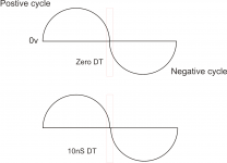
Hi,
This will help, see the picture🙂
Regards
MANOJ
Attachments
It definitely turns on the the body diode of the opposing switch. This is the conduction path during dead time or when the opposing switch is not turned on.probably turning on the body diode of the opposite
switch. .
It takes a finite time to turn on or off a device, especially mosfets, as their gates are effectively capacitors, and it takes time to charge/discharge a capacitor.
Dead time allows for the charge/discharge times.
Thank you for that. When I read that a little light went off. I guess I kind of knew about input capacitance of mosfets but that simple description really made it clearer to me.
Thanks for trying to explain - sorry but it has not really helped. I still have no idea how the PWM output stage actually works. What i need is for someone to explain in detail how the PWM waveform at the output maps onto a cycle of input waveform. I though i knew but obviously i don't, and i cannot understand the explanations. But thanks anyway.
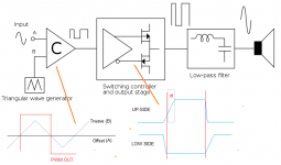
Just imagine a simple comparator.
At one input you apply a triangular signal.
To the second input you feed the audio signal.
The resulting output of the comparator is the typical PWM pattern of class D amps.
Also in self oscillating types you will end up in the same output PWM pattern.
For the resulting PWM pattern it does not matter if the triangle/carrier is generated seperately or by the feedback loop.
Just imagine a simple comparator.
At one input you apply a triangular signal.
To the second input you feed the audio signal.
The resulting output of the comparator is the typical PWM pattern of class D amps.
Also in self oscillating types you will end up in the same output PWM pattern.
For the resulting PWM pattern it does not matter if the triangle/carrier is generated seperately or by the feedback loop.
I have no trouble understanding the basic principle of turning an analogue input signal into a PWM stream. Its what happens at the output that confuses me, and in particular the split rails and dual output devices.
I had assumed it functioned in a similar way to a a so called class AB (or class B) analogue output, where each device handled half of the waveform, the positive connected output device conducting during the top half of the waveform, and the negative connected output device handling the bottom half.
I assumed therefore that dead time in a Class-D amp happened during the zero crossing part of the input signal, when the output stage transitioned from the positive rail to the negative rail, etc.
In a class AB analogue amp, this transition causes crossover distortion, but there is no intrinsic problem with both devices being on at the same time (as they are in a properly biased class AB amp), since this only occurs during the zero crossing interval when the signal is at a low level and the devices are conducting low levels of current.
Why i had problems understanding dead time in a Class D amp, was that if it worked as i had supposed, and that switchover from one rail to the other only happened ever zero crossing of the input, i could see no reason for dead time during the handover, since relatively huge amounts of "dead time" occur between pulses anyway as part of the mark-space nature of the PWM stream, and because it seemed to me that the pulses would be at there shortest with a low level signal.
Apparently this is not how it works - although i confess i can see no reason why it could not work this way. I will continue to try and imagine various ways in which this might work, until i hit on something which makes sense.
During the Crossover Switching point in a Class AB amp the output devices are only slightly conducting and present a considerable amount of ON resistance, Therefore only a little amount of current flows through the top and bottom devices.
In a Class D setup the devices are switched fully on (hard) and the devices present a very very small amount of resistance (Rsdon), About as much as a piece of plain wire for an FET.
So if they are on at the same time (no dead time) this forms a complete short between the two supply rails and the supply will try to deliver all of the current it possibly can at this time.
If it exceeds the rating of the output devices (FET's) then it will destroy one or both of the devices.
There is no way around this and is why a dead time must be incorporated during the Crossover Switching point.
I hope this helps you to understand better.
jer 🙂
Thanks for trying to explain - sorry but it has not really helped. I still have no idea how the PWM output stage actually works. What i need is for someone to explain in detail how the PWM waveform at the output maps onto a cycle of input waveform. I though i knew but obviously i don't, and i cannot understand the explanations. But thanks anyway.
Ok.
These arent the actual values in a class D system but just examples. The switching frequencies are often very high.
(The Classic-D sub amp i have runs at around 500khz)
Imagine a square wave of 1000hz at 100 volts.
Each cycle positive is 50 volts above earth.
Each cycle negative is 50 volts below earth, or -50 volts.
It swings positive and negative 1000 times a second.
Each time it swings positive, it stays positive for 500us, it then swings negative for 500us, and then back again.
so 500us of 50 volts plus 500us of -50 volts = 0 volts. the average is 0 volts.
ok, so we have an audio signal come in thats say.. 1 volt positive. (this is after a gain stage)
What will happen is that the signal will spend say.. 550us positive, and 450 us negative. That difference is called the "mark/space ratio"
Because the output now sees a bit more time positive then negative, the output is actually above earth now, as the filter spends more time connected to the positive rail.
How does it do this?
The amp creates a very accurate sawtooth wave at 1000hz. Once again its average is zero.
The amp compares this sawtooth wave with the input signal.
Since a sawtooth wave is symmetrical, (50 percent positive, 50 percent negative), if you compare this sawtooth wave with zero volts, it will output a signal thats 50 percent of the time positive, and 50 percent of the time negative. Basically saying "im HIGH for 500us, then im LOW for 500us). Literally, just high/low/high/low.
That output is now a square wave. 500us HIGH, 500us LOW.
Its mark space ratio is 1:1 because those times are the same.
If the input is now 1 volt positive, that comparator will create a square wave (well, now actaully a rectangular wave) with say 450us high and 550 us low, because the switching point is now higher in that sawtooth waveform. It will switch HIGH later, and LOW earlier, making it spend more time LOW then high.
The class D output stage mosfets duly amplify that ON/OFF to say 100 volts +/- and feed it through a low pass filter.
That output is now a pretty close replica of the input, just higher in current/voltage.
Now, lets go back to the pure square wave. ON/OFF/ON at a regular interval.
Now, dead time is put in because that mosfet power stage having capacitors as the mosfet gates take time to turn on and off.
Turning a mosfet on involves charging/discharging its gate. It takes time, and you are charging through a resistor. Its a natural RC circuit with a time constant.
What this means is that if you feed a 500us pulse to a mosfet, it may actually take 1us to turn on and 2 us to turn off.
Hence, the actual output is 501us seconds long.
So you have a short between source and drain for 501us, giving a 501us on time.
So the upper positive mosfet is on for 501us of a 500us signal.
And the bottom mosfet is on for 501us for the other 500us signal.
Now there is an overlap of 1us when BOTH mosfets are on.
Thats a direct short between positive and negative for 1us. Which is plenty of time to explode.
Dead time forces the output signal to delay turning on/off for a few us. tiny amounts, but it means in the end, a 500us/500us square wave actaully turns the mosfets gate drivers on in turn for 409us each. Giving us 500us ON time in each mosfet.
That time between when neither are active is the dead time. Its designed to be as small as possible, but not at any stage where there is a possibility of a short between the amp rails.
The issue with deadtime compared to cross overdistortion is that crossover distortion occurs as both transistors are in the low current switching area, just as one starts to turn on, the other is just turning off, this is around the zero volts area. Both transistors at this stage arent turned on hard at all, so only a very small current flows between them.
With a square wave output of a class D amp there IS no time when both are in a low current position, they are either ON or OFF.
So thats 100 volts!
If both are ON at the same time, its a dead short, if both are OFF, their is no current source/sink for any current flowing in the output stage filter and speakers, which is bad as well, hence the aim to get fast as possible mosfet switching times, (this means gate charge currents of over an amp)
As for how the switching creates an audio output?
Imagine turning on and off a light really quickly. like... so quick you cant see it flicker. It will look "dim" to the eyes, even though the current is going on/off/on/off the lamp and your eyes "Average" it. Creating a low pass filter.
In effect, a Class D amp is really a Switch Mode PSU!!!
It just happens to be able to change its output voltage really fast that by some pure chance and magic happens to correspond to the audio input 🙂
Last edited:
For 1Khz one full cycle is 1000us and each half of the waveforms time period is 500us not 50us.
I think you just have your decimal pace in the wrong spot is all.
If you were talking about 10Khz then 50us would be correct for one half of the cycle. 🙂
jer 🙂
I think you just have your decimal pace in the wrong spot is all.
If you were talking about 10Khz then 50us would be correct for one half of the cycle. 🙂
jer 🙂
- Status
- Not open for further replies.
- Home
- Amplifiers
- Class D
- what is dead time?