Hi!
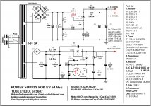
Could somebody tell me how to adjust this circuit for lower output voltage??
e.g. 180Vdc and 100Vdc? It has now 270Vdc on the output. (info from Andrea Ciuffoli"s great site)
Greets:
Tyimo
Could somebody tell me how to adjust this circuit for lower output voltage??
e.g. 180Vdc and 100Vdc? It has now 270Vdc on the output. (info from Andrea Ciuffoli"s great site)
Greets:
Tyimo
Attachments
Last edited:
Since zener diode D5 is a voltage clamp which protects MOSFET Q1's gate-to-source thin oxide, I would have expected that Q1's source would be on the output side (connected to R6), while Q1's drain would be on the input side (connected to R1).
However the schematic is drawn the other way, with Q1's source = input, and Q1's drain = output, and clamp diode D5 from gate to drain. Jeepers!
However the schematic is drawn the other way, with Q1's source = input, and Q1's drain = output, and clamp diode D5 from gate to drain. Jeepers!
Yes, but I don't know what do you want to say????However the schematic is drawn the other way, with Q1's source = input, and Q1's drain = output, and clamp diode D5 from gate to drain.
please , complete this completely non-commercial survey and then you can see our circuit , without deliberate errors


Hi,
This circuit can work without any changes from 100V to 350V
to support 450V voltage use IRF840
This circuit can work without any changes from 100V to 350V
to support 450V voltage use IRF840
Hi!
Thanks!
Do I need to adjust or change some value if I need to get 180Vdc?
What should be the input Vac in this case? I don't know the voltage drop of your circuit.
Merry Christmas!
Tyimo
Thanks!
Do I need to adjust or change some value if I need to get 180Vdc?
What should be the input Vac in this case? I don't know the voltage drop of your circuit.
Merry Christmas!
Tyimo
If the DC voltage on C5 is 200V
Vout = 200 * ( R2 / ( R2 + R1 )) - Vgs = 200 * ( 100K / ( 100K + 22K)) - 4 = 200 * 0.82 - 4 = 159V
about VAC = 1.2 + 200 / 1.41 = 143V
Vout = 200 * ( R2 / ( R2 + R1 )) - Vgs = 200 * ( 100K / ( 100K + 22K)) - 4 = 200 * 0.82 - 4 = 159V
about VAC = 1.2 + 200 / 1.41 = 143V
VAC = 160V
VC5 = 224V
VOUT = 179V
The final output voltage depend in part by the current so probably you need to adjust R1 or R2.
VC5 = 224V
VOUT = 179V
The final output voltage depend in part by the current so probably you need to adjust R1 or R2.
virtual battery , all the way from time of Technics coining da name , is just fancy name for cap multiplier , with added resistive divider for establishing output voltage range
in other words - neither proper cap multiplier nor proper reg
in other words - neither proper cap multiplier nor proper reg
- Status
- Not open for further replies.
- Home
- Amplifiers
- Power Supplies
- Virtual Battery PSU