I have drafted a class d amplifier with a minimum of standard devices.
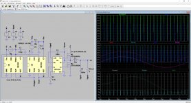
The PWM consists of 2 rectangle generators, each based on a timer IC NE555 (U1, U2) working with the same current regulator diode E-102 (I1) and the same capacitor (C1).
The first timer (U1) is in astable mode, generating the trigger signal with a frequency of 500 kHz for the second timer. The second timer (U2) is in voltage controlled monostable mode. It converts the signal voltage (V4) into a pulse width.
In a stereo amplifier the first timer is only needed once, because it can trigger the monostable timers of both channels.
The pulse width modulated signal is fed into the input of a half bridge driver (LM5104) which controls the gates of the power output stage (M1, M2). A low pass filter (L1, C4) with a roll off frequency of 40 kHz converts the amplified PWM signal into a continuous voltage at the load resistor (Rload).
What do you think about this design?
Attachments
Last edited:
Hello,
there are many samples for working Class D amplifier
Reference Designs are for free from semiconductor suppliers
NE555 is not solution for Audio and fun for school project
there are many samples for working Class D amplifier
Reference Designs are for free from semiconductor suppliers
NE555 is not solution for Audio and fun for school project
Indeed, my intention is to learn functional principles by doing things the very basic way and not with special devices.
Relating to the NE555 timer IC. Where do you see issues with it in audio?
This device implements very fast comparators which are useful to operate with higher PWM frequencies. In order to get the required linearity for the PWM over a wide range of input voltages the use of a current regulator diode (constant current source) as the charging device for the capacitor is crucial.
design change
Hi @ all,
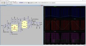
meanwhile my idea went through a redesign to make it even more simple.
I've found a useful analog to pwm converter device from Analog Devices LTC6992 which I implemented as U1 in my schematic. Only one external resistor R3 is needed to set its pwm frequency. It converts each signal voltage between 0 and 1V at its input into a linear pwm signal from 0 to 100% duty cycle on its exit. So only a voltage devider R1, R2 is needed to set the average input voltage to 0.5 V in order to get an idle output duty cycle of 50 per cent.
The half bridge driver,and the the power MOSFETs have not changed. The output low pass filter is redesigned to roll-off at 40 kHz.
The circuit design allows still the full exchange capability for all its modules in order to adapt the circuit to different power requirements.
Hi @ all,
meanwhile my idea went through a redesign to make it even more simple.
I've found a useful analog to pwm converter device from Analog Devices LTC6992 which I implemented as U1 in my schematic. Only one external resistor R3 is needed to set its pwm frequency. It converts each signal voltage between 0 and 1V at its input into a linear pwm signal from 0 to 100% duty cycle on its exit. So only a voltage devider R1, R2 is needed to set the average input voltage to 0.5 V in order to get an idle output duty cycle of 50 per cent.
The half bridge driver,and the the power MOSFETs have not changed. The output low pass filter is redesigned to roll-off at 40 kHz.
The circuit design allows still the full exchange capability for all its modules in order to adapt the circuit to different power requirements.
Attachments
Hi Gunter,
A good initiative that will bring you fun and knowledge. It will not result in a product that can be sold - very little can beat a TPA3116 "value for money"-wise. Constructing your own circuit, even if not economically competitive, will force you to think about the parameters that are important for good sound. That is the way to understand electronics.
Carry on!
Its got bad shoot-through(*), and requires tons of decoupling. The CMOS versions like the 7555 are way better in most respects, I recommend trying a comparison.Relating to the NE555 timer IC. Where do you see issues with it in audio?
The 555 has a push-pull bipolar output driver which during transitions allows pulses of current to flow directly between supply and ground, of the order of several 100mA... In other words its an EMI generator that needs work to tame when near sensitive signals.
Have you looked at building a delta sigma modulator based design? Delta-sigma modulation - Wikipedia
Run your model with an input signal of 1KHz over 2mS to 7mS and add a .four 1K V(Vo2) spice directive. View the spice error log to see the distortion figures.
Its got bad shoot-through(*), and requires tons of decoupling. The CMOS versions like the 7555 are way better in most respects, I recommend trying a comparison.
The shoot-through happens at a current of 200 mA within a time interval of about 10 to 20 ns. You can easily avoid conducted and radiated emissions by use of a 100 nF Capacitor with short connection to the power rails of the IC.
The CMOS versions of NE555 have unfortunately limited functional compatibility to the bipolar original. So their cv-Input doesn't work between 0 and VCC/3. this is due to their very different input stage design. It is possible to solve this problem by use of a circuit add-on between out and thresh which limits the discharge of the capacitor to VCC/3.
Have you looked at building a delta sigma modulator based design? Delta-sigma modulation - Wikipedia
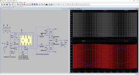
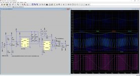
Yes I did. It works, also with relatively low effort. This is still an old circuit design without a half bridge driver and with a complimentary MOSFET output stage. But it can surely substituted by the driver / output stage design of my recent draft.
Attachments
Have you looked at building a delta sigma modulator based design? Delta-sigma modulation - Wikipedia
I have modified the circuit design of the sigma-delta converter by use of current regulating diodes E-102 in order to get more linearity. Furthermore I have added the half bridge driver, the power MOSFETs and the low pass filter of my other class d design.
Attachments
Very good. Makes me want to start up LTSpice today. The low parts count is great, and you have an amplifier with an analog or digital input (DSD density stream).
I may have to dig around in my parts bins to see what I can build.
I may have to dig around in my parts bins to see what I can build.
Fine. I still fail to see what your purpose is here. You publish pictures of LTSpice circuits without providing.asc and supporting files for others to investigate performance, fail to provide details of such performance yourself and reject out of hand suggestions as to how to improve that performance as being too complex. Given you like simplicity why not throw away the 555 and the other stuff and put a HCMOS inverter on the input of the LM5104 to get delta sigma then publish some more pictures with no performance figures and no .asc or supporting files for others to play with.
- Home
- Amplifiers
- Class D
- very simple class d amplifier made of standard devices