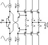
The new version of the “common base input..." (https://www.diyaudio.com/community/threads/common-base-input-for-power-amplifier.387450/) amplifier includes a new design of the output stage to make possible the use of vertical mosfets (IRFP240/IRFP9240). The figure below shows a simplified version of the relevant part of the circuit. The output is adjusted by sensing the current into the ballast resistors using properly biased bipolar transistors (those shown in the simplified schematic). The 4 rightmost mosfet devices in the figure are the ones actually doing the voltage drive into the speaker and operate in open loop. It was done this way to minimize current spikes in the crossover region. As mentioned in my previous post the prototype works as expected and a final thermal stability test was done leaving the amplifier operating for several hours at 60% of max power. Originally the bipolar transistors (common base) were attached to the heat sink in close proximity to the output devices to provide thermal feedback, but it was removed due to a very slow thermal oscillation that I considered an open door to thermal runaway. Considering that the bias current is sensed on the resistors (and not on gs+resistor as usually done) there is still a significant amount of thermal feedback: if the temperature of one of the output transistors increases, current will increase in all devices due to a reduction of the threshold voltage, that increase is sensed by the current control loop that in turn will force the gs voltage (in all mosfets) to get reduced in order to maintain that current constant. The problem is, I have no way (given my skills) to demonstrate that the circuit is thermally stable. I would appreciate any help regarding how to predict thermal stability (or instability!).
Attachments
Complementary parts like IRFP 240 and IRFP 9240 do sound very different. The ear does detect, listen.
Result is an impure sounding amp. Everytime.
Result is an impure sounding amp. Everytime.
I bet having perfect ears is a curse.Complementary parts like IRFP 240 and IRFP 9240 do sound very different. The ear does detect, listen.
Result is an impure sounding amp. Everytime.

If you use enough gNFB, you shouldn't hear any difference?
If I was building an SS amp, I'd go quasi-complementary AKA NPN only like a tube amp.
If I was building an SS amp, I'd go quasi-complementary AKA NPN only like a tube amp.
;-)I bet having perfect ears is a curse.
Differences does the ear detect: the simpest proof: connect channel-different ("double-mono") psus;-) May be the start into highend;-)
No proof: no experience: no quality;-)
For those of you interested in the thermal behavior of a power amplifier and ways to verify performance with respect of thermal stability I have this LTspice simulation that seems to reflect up to a point actual performance. Each power device (IRFP240/IRFP9240) are modeled as a combination of the device itself and a controlled voltage source in series with the source terminal to emulate the threshold voltage dependence on junction temperature. The voltage shift is simulated by applying a voltage equal to the estimated junction temperature on the Voff pin. In this example a -2mV/C is assumed.The new version of the “common base input..." (https://www.diyaudio.com/community/threads/common-base-input-for-power-amplifier.387450/) amplifier includes a new design of the output stage to make possible the use of vertical mosfets (IRFP240/IRFP9240). The figure below shows a
The junction temperature is estimated using a "bi" current source using the formula I=V(Re)*(Vcc-Vsd), where Re is the ballast resistor on each power MOS source. The current is scaled and filtered using appropriate resistors and capacitors as shown in the far right of the schematic. The rest of the schematic emulates in very simplified form the voltage amplifier that precedes the power section. The plots show temperature (as a voltage in the plot) for 3 cases:
1.- complete thermal feedback from the power devices (4 leftmost devices) into the 2 devices operating with constant current (M1,M2).
2.- partial thermal feedback (1/2)
3.- no feedback (represents M1 and M2 thermally isolated from the current carrying power devices).
in cases 1 and 2 the temperature (and bias current) gets stable, in case 2 at a higher temperature. In case 3 current increases with no apparent limit.
It is consistent with the criteria that. for temperature runaway to occur not only positive feedback is required, but the gain of the loop has to be more than one. To determine the loop gain with precision looks to me as very difficult undertake. But a simulation as shown can help to determine the risk of a given implementation.