I'm looking for advice and tips related to PCB board layout and signal+ground trace/track routing.
I'm designing an analog-only PCB that has several I/O signals leading to and from other boards and several analog amplifier ICs. I have some questions about how and where I need to use ground tracks to carry the return current, and how I can best arrange these on the board to reduce noise and hum (EMF) pickup. I'm using star grounding and no ground plane on the board.
From what I have generally come to understand, you want to run signal and return tracks close to each other. To me this seems the same logic used when running cables off the PCB, e.g. between boards. I'm unclear about what happens with signal currents on the board, especially when ICs are involved. For instance, I can run a ground return from the star ground system along the signal track out to the board edge where the I/O connector is located, but it's not always possible to run this signal+return pair all the way up to where the signal trace connects to a pin on the IC. Should this be of much concern? Likewise, should I try to follow the signal+return principle for tracks that go between ICs on the same board? If so, how do I figure out where the return current is flowing? Does the current "return" to the ground pin of the first IC, or does it flow back to the star ground system? Does it make any sense to run a "spur" ground track, meaning one that runs along the signal track but then stops where the paired signal track reaches an IC pin, e.g. that end is left disconnected. The other end would be connected to the ground system. I can't convince myself that this would be effective as a "return" and current would flow, since one end is disconnected.
I have not been worried about this in the past, and I have designed boards that seem to have relatively low noise, etc. but I have always been curious about on-board routing. I'm completely self-taught so any words of advice would be very much appreciated. I have read many PCB design guideline type documents that I could find on the web, but none seem to address this particular issue - low noise analog signal routing. Maybe its just not all that important?
Yes.I'm looking for advice and tips related to PCB board layout and signal+ground trace/track routing.....................From what I have generally come to understand, you want to run signal and return tracks close to each other.
Have you read Tomchr chipamp Thread? trace routing turned out to be critical to trying to match the discrete wiring prototype. In the end he IMPROVED the PCB version to better than National specifications, which came as a surprise to me and him.To me this seems the same logic used when running cables off the PCB, e.g. between boards. I'm unclear about what happens with signal currents on the board, especially when ICs are involved. For instance, I can run a ground return from the star ground system along the signal track out to the board edge where the I/O connector is located, but it's not always possible to run this signal+return pair all the way up to where the signal trace connects to a pin on the IC.
Try to identify the ROUTE that the SOURCE uses for it's Flow and Return. All current MUST RETURN to the Source. The IC can be so small that the route inside the chip can be assumed to run from pinIN to pinOUTShould this be of much concern? Likewise, should I try to follow the signal+return principle for tracks that go between ICs on the same board? If so, how do I figure out where the return current is flowing? Does the current "return" to the ground pin of the first IC, or does it flow back to the star ground system? Does it make any sense to run a "spur" ground track, meaning one that runs along the signal track but then stops where the paired signal track reaches an IC pin, e.g. that end is left disconnected. The other end would be connected to the ground system. I can't convince myself that this would be effective as a "return" and current would flow, since one end is disconnected.
Marce and co. have given many words of wisdom and many links to papers that give some answers and some explanation.I have not been worried about this in the past, and I have designed boards that seem to have relatively low noise, etc. but I have always been curious about on-board routing. I'm completely self-taught so any words of advice would be very much appreciated. I have read many PCB design guideline type documents that I could find on the web, but none seem to address this particular issue - low noise analog signal routing. Maybe its just not all that important?
However, much of this is directed to VHF/UHF and thus utilises multi-layer PCBs where layer to layer distances are <10mil/thou.
But the same practical routing can be applied to audio frequencies. Even using single layer and two layer PCBs with 60mil/thou layer spacing.
http://www.x2y.com/filters/TechDay0...log_Designs_Demand_GoodPCBLayouts _JohnWu.pdf
including pretty pictures.
A ground plane is best for precision analogue design...Or for ultimate resolution balanced routing (still with a ground plane).
Funnily enough I am doing a sensitive analogue board now, analogue front end DSP then a digital section (oh and a few ADC/DACs to add a bit of spice, 3,000 connections 4,000 pins) great fun. We are splitting the grounds into AGND DGND
If you can put up a schematic...I will explain balanced (or differential routing in more detail later, just on dinner break now).
Last edited:
The spur will not have current flow. What sort of effect could it have?
Antenna...single ended spurs are effectively an antenna structure and will pick up/radiate noise.
follow the current...
This is EXACTLY what I am trying to figure out. By the way thanks for the detailed reply.
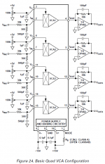
The general circuit I am implementing is shown in the attachment. It's taken from the datasheet of an SSM2164 quad VCA. I'm connecting it to single ended inputs, with the addition of ground loop breaking resistors on the signal return (shield/ground) lines.
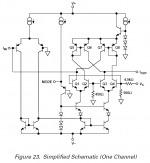
As Andrew mentioned, in order to pair source and return you have to know where the current is flowing, including into, through, and out of the IC. The IC is so small that the "through" part is not important. You know exactly what pin that the input signal connects to. The question remains: WHERE DOES THE INPUT CURRENT GO? I have also attached the internal (simplified) VCA schematic that should show this. There are really only a couple of possibilities: input current is either flowing "out" to ground, or out one or both of the rails. Which is it???
Looking at the simplified internal circuit for the VCA (it's for one channel), you can see that there is a single input pin, shown at the left. The remaining pins are ground(s) and the V+ and V- rail pins. Unfortunately I don't really have a clue how to figure out how current is flowing through this topology and where it goes.
Can someone please take a look at the internal circuit and let me know if you can identify where input current exits the circuit? I think that once I know this, how adn where to route the return track will be clear.
Try to identify the ROUTE that the SOURCE uses for it's Flow and Return. All current MUST RETURN to the Source.
This is EXACTLY what I am trying to figure out. By the way thanks for the detailed reply.
The general circuit I am implementing is shown in the attachment. It's taken from the datasheet of an SSM2164 quad VCA. I'm connecting it to single ended inputs, with the addition of ground loop breaking resistors on the signal return (shield/ground) lines.
As Andrew mentioned, in order to pair source and return you have to know where the current is flowing, including into, through, and out of the IC. The IC is so small that the "through" part is not important. You know exactly what pin that the input signal connects to. The question remains: WHERE DOES THE INPUT CURRENT GO? I have also attached the internal (simplified) VCA schematic that should show this. There are really only a couple of possibilities: input current is either flowing "out" to ground, or out one or both of the rails. Which is it???
Looking at the simplified internal circuit for the VCA (it's for one channel), you can see that there is a single input pin, shown at the left. The remaining pins are ground(s) and the V+ and V- rail pins. Unfortunately I don't really have a clue how to figure out how current is flowing through this topology and where it goes.
Can someone please take a look at the internal circuit and let me know if you can identify where input current exits the circuit? I think that once I know this, how adn where to route the return track will be clear.
Attachments
The current has to go back to the Source.The question remains: WHERE DOES THE INPUT CURRENT GO?
This is fundamental to ALL CIRCUITS.
When considering the Output to Load, the current has to come back to the chip, since this was the Source.
When considering the PSU, the current going to the chip must return to the PSU, the PSU is the Source.
Consider each circuit individually . Find the source then imagine the route for Flow and where you can place the Return.
When considering the PSU, the current going to the chip must return to the PSU, the PSU is the Source.
Consider each circuit individually . Find the source then imagine the route for Flow and where you can place the Return.
The current has to go back to the Source.
This is fundamental to ALL CIRCUITS.
Sure, sure, that much is well understood. Repeat this mantra 1000 times. Any enlightenment? No. It's the relative PATHS of the send+return that is important where noise and hum pickup is concerned. My question pertains to ROUTING on the PCB to keep the paths close and loop area low.
For my circuit implementation, the question is more about what pin of the IC the input current flows out of, and how it returns back to the source. For instance, if it flows out the ground pin, then I should take care to route that trace along side the signal line wherever possible, to keep the loop area low. This would be better than running the ground back to the star point and then back again to join the signal wire at the edge of the board. That ground path, combined with the signal path, would form a loop. Likewise, if the current is flowing to one or the other (or both) rails, through the caps of the PS, to ground and then out to the board edge I need to think about how to best route all these paths/tracks.
When considering the Output to Load, the current has to come back to the chip, since this was the Source.
When considering the PSU, the current going to the chip must return to the PSU, the PSU is the Source.
Consider each circuit individually . Find the source then imagine the route for Flow and where you can place the Return.
I understand the output current flow well, so that isn't the concern here.
Saying that the input current flows to the PS is still a bit too general. The PS is comprised of two rails and ground. Where, SPECIFICALLY, does the input current go?
What is the exact path from the IC to the board edge to the shield/return connector? Does it go through the PS or just via ground?
Can anyone say where the input current goes exactly - at what pin or pins does it emerge on the IC? There are only three possibilities: the ground pin, Vcc, or Vee. Bonus points if you can explain the input current flow in the simplified VCA (internal) circuit.
Current flows from the most positive point on a circuit to the most negative point... presuming there's a path; and if there isn't a path, then that point's not part of the circuit.
An IC may not have a GND pin. Current can flow into and out of both inputs and outputs.
Decoupling caps are placed across the power pins so as to minimize the loop area of the circulating currents, because the AC components in the power drain are seen as being short-circuited by the capacitance. It's like these AC currents have a life of their own, and they do, momentarily, they're transients. You can look at this as the decoupling cap acting as a reservoir, but the AC/SC model is much more instructive in terms of EMC. In a single-sided circuit, one side of the decoupling cap is grounded.
If the circuit is (+ve) single sided, then GND is the most negative point. Otherwise ground is irrelevant other than to the input, output and feedback networks, and the PSU.
Current flows from the most positive point on a circuit to the most negative point... presuming there's a path; and if there isn't a path, then that point's not part of the circuit.
An IC may not have a GND pin. Current can flow into and out of both inputs and outputs.
Decoupling caps are placed across the power pins so as to minimize the loop area of the circulating currents, because the AC components in the power drain are seen as being short-circuited by the capacitance. It's like these AC currents have a life of their own, and they do, momentarily, they're transients. You can look at this as the decoupling cap acting as a reservoir, but the AC/SC model is much more instructive in terms of EMC. In a single-sided circuit, one side of the decoupling cap is grounded.
If the circuit is (+ve) single sided, then GND is the most negative point. Otherwise ground is irrelevant other than to the input, output and feedback networks, and the PSU.
Thanks for posting that. I hadn't thought about it that way, but it makes sense. So, in general, currents enter through the Vcc (V+) pin and exit through the Vee (V-) pin of most ICs? This would include additional currents "entering" through the input pin(s) - they flow to and out the Vee pin?
The main source of hum in an amplifier is at smoothing capacitors.
The charging impulses modulate the ground line.
I got seriously caught out with a mixer.
I just mixed in audio ground with power supply ground and got 1 volt of hum on the output !
On my next pcb revision I completely separated the audio and power supply grounds and they met at a star point once. This time the output was silent.
Anywhere there is any power you can get modulation of the ground line.
I found with low power signals I didn't get any problems.
Current flows from the most positive point on a circuit to the most negative point... presuming there's a path; and if there isn't a path, then that point's not part of the circuit.
An IC may not have a GND pin. Current can flow into and out of both inputs and outputs.
Decoupling caps are placed across the power pins so as to minimize the loop area of the circulating currents, because the AC components in the power drain are seen as being short-circuited by the capacitance. It's like these AC currents have a life of their own, and they do, momentarily, they're transients. You can look at this as the decoupling cap acting as a reservoir, but the AC/SC model is much more instructive in terms of EMC. In a single-sided circuit, one side of the decoupling cap is grounded.
If the circuit is (+ve) single sided, then GND is the most negative point. Otherwise ground is irrelevant other than to the input, output and feedback networks, and the PSU.
On SINGLE ENDED SIGNALS the ground is the reference and the current flows via the GND, decoupling capacitors should be placed between supply pins and the GND, not between the power pins.
How many devices don't have a GND pin.
Last edited:
Thanks for posting that. I hadn't thought about it that way, but it makes sense. So, in general, currents enter through the Vcc (V+) pin and exit through the Vee (V-) pin of most ICs? This would include additional currents "entering" through the input pin(s) - they flow to and out the Vee pin?
NO...wrong. Current is referenced to GND with single ended signals.
For a start audio signals are a.c. so current flow is not in one direction. Input current does NOT flow into the device and out the neg. supply pin, it is a.c. the current flows in and out of the input pin.
Current flow is not lots of electrons whizzing around the circuit like a train on a track, (electrons move at about 1m per hour) it is the electromagnetic wave that moves at a speed (a speed slower than the speed of light, roughly 50% the speed of light on a PCB). With audio signals being a.c. current flows in and out of the input pin, it is not a one way journey.
Last edited:
Here's a bit of light reading, unfortunately there is no easy explanation for all this, but getting to grips with the basics of signal flow will help. Have fun...there 's plent more but I have tried to pick the simplest and most illustrative, one of the best being the John Wu presentation I linked earlier.
A good primer for grounds page 12.54
http://www.analog.com/library/analogdialogue/archives/43-09/edch 12 pc issues.pdf
An excellent reference from one of the real ground Gurus
http://www.hottconsultants.com/pdf_files/ground.pdf
Bill Whitlock AES presentation...
http://centralindianaaes.files.wordpress.com/2012/09/indy-aes-2012-seminar-w-notes-v1-0.pdf
How currents flow and return current distribution, plus more on "grounds"
http://sites.ieee.org/ctx-emcs/files/2010/09/Archambeault-Ground-Myth.pdf
http://www.ewh.ieee.org/soc/emcs/acstrial/newsletters/spring08/design_tips.pdf
http://www.emcs.org/acstrial/newsletters/fall08/tips.pdf
Successful PCB Grounding with Mixed-Signal Chips - Follow the Path of Least Impedance - Tutorial - Maxim
http://www.icd.com.au/articles/EM_Fields_Pt1_PCBDesign-Mar2013.pdf
Calculating PCB track Impedance...There are many calculators online or Saturn PCB toolkit to do the hard work.
http://www.polarinstruments.com/support/cits/IPC1999.pdf
Saturn PCB Design - PCB Via Current | PCB Trace Width | Differential Pair Calculator | PCB Impedance
When I get chance I will go through my documents and get more info as I have Tis analogue newsletters and similar from National Analog Devices etc.
Just found this, a good illustration of an input loop, even though its leads it could be traces on a PCB:
http://www.analog.com/static/imported-files/rarely_asked_questions/groundNoiseMeasurement.pdf
Last edited:
On SINGLE ENDED SIGNALS the ground is the reference and the current flows via the GND, decoupling capacitors should be placed between supply pins and the GND, not between the power pins.
How many devices don't have a GND pin.
Many devices don't have a ground pin. That's what I said.
If you're going to disagree with me, do me the courtesy of reading what I wrote.
I'm talking about single-sided power supplies, not single sided signals. That's what I mean when I say :- If the circuit is (+ve) single sided, then GND is the most negative point. One of the power pins is connected to ground.
You should read Doug Self on the decoupling of (NE5532) opamps, and the danger of coupling noise into the ground system with the schema you outline, and take a look at the decoupling in his NE5532 opamp poweramp.
Overall distributed capacitance will comprise some larger electrolytics to both rails from ground, but 100+100nF between the rails with a grounded centre tap just decouples the rails at HF that bit less effectively than 1 from rail to rail.
Maybe its just not all that important?
In general electronics, signal integrity only has to be good enough. It's more likely to be an EMC issue anyway. In audio it's never good enough, except that it's always OK in listening impressions.
Industry anticipates test and respin. Of course amateurs can test and respin too, it's just a question of cost. You might wonder why they would, considering the evident lack of testing in so many commercial audio products, however.
Unfortunately layout can require thinking. It's not always that dreamy kind of daze where you shuffle components around and draw the tracks willy-nilly with the only object being achieving connectivity somehow, and when the last connection in the ratsnest is gone, you're done. It can be like that for a PIC circuit, or some non-critical analog stuff, but a SMPS may refuse to function, unlike a linear, which may have degraded performance, but will probably still 'work' regardless of how the ground connectivity is achieved. Many larger companies have an extensive library of previous tested designs available as a basis for modification, easing the burden on the layout engineer.
4 and 7 layer boards are commonplace in telecoms applications, buried tracks and a plane for each power rail mean that maintaining integrity even when exposed to a blast of high-power external broadband radio noise becomes less of an impossibility.
Many mixed signal devices (DACs, volume controls) and analog devices (TPA6120A, chip amps) do have GND pins, and many have explicit instructions about how their power pins are to be decoupled. It's important to follow these recommendations, but not slavishly. They can be wrong.
The currents circulating in the input networks are trivial. That's why the amplifier is there. We just don't want any big currents near them, so we don't want them on the board to the extent that we can keep them off, so if we have e.g. an RF input filter, then it's GND connections would be made to the input GND connection.
The feedback networks as a generality similarly carry small currents and so may share a trace connecting the input to the PSU GND.
The currents in the output may be non-trivial. This is where the bulk of current (other than the quiescent current) flows. The NETT current is zero in a dual-rail system. The return from the driven device (GND) should be directly connected to a robust junction physically equidistant from the PSU output caps where they share GND, or where PSU GND comes onto the board, where you'd expect to see a couple big electrolytics.
Power requirements and signal level increase (in general), from the front end of an amplifier to the output. This means that the power traces (and GNDs) should connect from most powerful to least powerful so that powerful devices are not pulling their power past lower power devices. Think how a tube psu powers the output tubes before the driver, before the input. Superimpose the rails in a dual-rail system, particularly class AB and B.
These are guidelines and as such are broad generalizations. Some may disagree with them on specifics.
There's no substitute for test, although simulation can tell you a lot, particularly if you can afford good tools, but even with what's free.
One other point. Very often there are other considerations, such as the positioning of sockets, displays or other controls. These can mean that a sub-optimal layout must be adopted, but this is in the nature of the trade-offs we accept for convenience of packaging or features. Modern devices have excess performance, so if you can't hear any hum or hiss, and it looks OK on RMAA then you have to make some progress, innit?
NO...wrong. Current is referenced to GND with single ended signals.
For a start audio signals are a.c. so current flow is not in one direction. Input current does NOT flow into the device and out the neg. supply pin, it is a.c. the current flows in and out of the input pin.
Current flow is not lots of electrons whizzing around the circuit like a train on a track, (electrons move at about 1m per hour) it is the electromagnetic wave that moves at a speed (a speed slower than the speed of light, roughly 50% the speed of light on a PCB). With audio signals being a.c. current flows in and out of the input pin, it is not a one way journey.
Not that you were trying to be patronizing in your response, but you are really dumbing this down a little too much with the train-on-track analogy!
Many devices don't have a ground pin. That's what I said.
If you're going to disagree with me, do me the courtesy of reading what I wrote.
You should read Doug Self on the decoupling of (NE5532) opamps, and the danger of coupling noise into the ground system with the schema you outline, and take a look at the decoupling in his NE5532 opamp poweramp.
Discussed on another thread regarding the Doug Self, as stated on that one pin to pin decoupling is only relevant on true differential signals.
Regarding the many devices don't have a ground pin, I read what you said and asked the question, I think you will find there are very few that don't have a ground pin, if any, I cant recall seeing any.
Maybe you should do some more research into this instead of just quoting one paper.
Last edited:
- Status
- Not open for further replies.
- Home
- Source & Line
- Analog Line Level
- understanding source+return current flow on PCBs