Hi all,
I've been given an old 70s Sony amp to try to repair (to learn), that has a series resistor (into the propriatory Sony module) visibly damaged.
I disconnected the 2 chip modules to ensure there's no damage to them. After several days of checking voltages and trying to understand, I've now discovered that a capacitor at the VAS stage has leaked fizzy electrolyte while I had it powered on.
I'm short on time at the moment, hoping to post some pictures, section of the schematic, and some of the voltages that I recorded later tonight.
I bought 2 of Self's books, trying to understand the various transistor stages before the Sony chips.
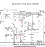
There is a current source PNP mirrored section that provides a current source to the differential amplifier stage at the input, and also it seems to provide current to the VAS stage, however I'm not sure how this works as there's a polarised electrolytic capacitor between the current stage and the VAS class A transistor amplifier. It seems different to anything I've seen in Self's books. Between the VAS stage and the Sony modules (SS050 I think they are), there is some sort of current protection system with 4 transistors, their bases being fed from the Sony modules.
Should the PNP transistor that provides the current source to the VAS stage always be on? The diode voltage drop of the other diode should be enough to lower the base voltage so it's less than the emitter and turn the transistor on?
The Emitter of the NPN transistor for the Class A is hooked up to the -36V rail via a 62 ohm resistor, so if this transistor is always on, it will surely punch more voltage across the capacitor in the middle than it can handle?
Quick summary:
Voltages on one channel seem fine. The other channel seems suspect.
Output relay protection is triggered and will not release.
Series resistor into one channel's Sony module is burnt to a crisp (colour of resistor has changed and DMM reads open circuit).
I did a diode test with the DMM on all the transistors (in-circuit) and they seemed fine (I think).
This 100uF / 6.3V electrolytic cap leaked.
Voltages from the collector of the PNP current source and the collector of the NPN class-A amp transistor was +36V DC and -36V DC, meaning there was some 72V DC across this 6.3V capacitor.
This surely means both the transistors were hard-on, allowing the +V and -V rails to be connected to the cap?
Various expected voltages from the schematic (roughly) match what I've probed other than the PNP collector / NPN collector voltage mentioned above.
There's a diode / capacitor in parallel from the +V rail to the bases of the 2 PNP mirror current sources - voltage there seemed to be slowly increasing or decreasing when I probed it (need to check my notes later on and report back).
I'm keen to try to diagnose this myself, in order to learn this "on my own", but would very much appreciate any sort of "cryptic" / "zen-like" questions or pointers you might have to "vaguely point me" into the direction that I can head to next.
I've been given an old 70s Sony amp to try to repair (to learn), that has a series resistor (into the propriatory Sony module) visibly damaged.
I disconnected the 2 chip modules to ensure there's no damage to them. After several days of checking voltages and trying to understand, I've now discovered that a capacitor at the VAS stage has leaked fizzy electrolyte while I had it powered on.
I'm short on time at the moment, hoping to post some pictures, section of the schematic, and some of the voltages that I recorded later tonight.
I bought 2 of Self's books, trying to understand the various transistor stages before the Sony chips.
There is a current source PNP mirrored section that provides a current source to the differential amplifier stage at the input, and also it seems to provide current to the VAS stage, however I'm not sure how this works as there's a polarised electrolytic capacitor between the current stage and the VAS class A transistor amplifier. It seems different to anything I've seen in Self's books. Between the VAS stage and the Sony modules (SS050 I think they are), there is some sort of current protection system with 4 transistors, their bases being fed from the Sony modules.
Should the PNP transistor that provides the current source to the VAS stage always be on? The diode voltage drop of the other diode should be enough to lower the base voltage so it's less than the emitter and turn the transistor on?
The Emitter of the NPN transistor for the Class A is hooked up to the -36V rail via a 62 ohm resistor, so if this transistor is always on, it will surely punch more voltage across the capacitor in the middle than it can handle?
Quick summary:
Voltages on one channel seem fine. The other channel seems suspect.
Output relay protection is triggered and will not release.
Series resistor into one channel's Sony module is burnt to a crisp (colour of resistor has changed and DMM reads open circuit).
I did a diode test with the DMM on all the transistors (in-circuit) and they seemed fine (I think).
This 100uF / 6.3V electrolytic cap leaked.
Voltages from the collector of the PNP current source and the collector of the NPN class-A amp transistor was +36V DC and -36V DC, meaning there was some 72V DC across this 6.3V capacitor.
This surely means both the transistors were hard-on, allowing the +V and -V rails to be connected to the cap?
Various expected voltages from the schematic (roughly) match what I've probed other than the PNP collector / NPN collector voltage mentioned above.
There's a diode / capacitor in parallel from the +V rail to the bases of the 2 PNP mirror current sources - voltage there seemed to be slowly increasing or decreasing when I probed it (need to check my notes later on and report back).
I'm keen to try to diagnose this myself, in order to learn this "on my own", but would very much appreciate any sort of "cryptic" / "zen-like" questions or pointers you might have to "vaguely point me" into the direction that I can head to next.
We need a model number at the very least 🙂 and the component references of the burnt up resistor.
Sorry @Mooly I was just getting ready to go out and running out of time 🙂
Sony STR-4800
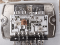
R763 I believe is the one that burnt (Right channel burnt, only left channel shown on schematic, which is R713 for Left).
C706 leaked.
Q754 is class A for Right channel, Q753 is at the top the current source for the VAS. There's a whole bunch of weird-looking (to my novice eyes) transistor arrangement that leads into the Sony SSA050 module for current protection.
Schematic shows +-37 for the supply but mine is +-36, maybe just mains is a bit lower?
Emmiter for the differential amp is at 0.8v rather than the 0.7v on the schematic.
With the modules in place, the 0v output that goes back to the feedback was hard at one of the supply rails - need to check my notes when I get back.
Thanks 🙂
Sony STR-4800
R763 I believe is the one that burnt (Right channel burnt, only left channel shown on schematic, which is R713 for Left).
C706 leaked.
Q754 is class A for Right channel, Q753 is at the top the current source for the VAS. There's a whole bunch of weird-looking (to my novice eyes) transistor arrangement that leads into the Sony SSA050 module for current protection.
Schematic shows +-37 for the supply but mine is +-36, maybe just mains is a bit lower?
Emmiter for the differential amp is at 0.8v rather than the 0.7v on the schematic.
With the modules in place, the 0v output that goes back to the feedback was hard at one of the supply rails - need to check my notes when I get back.
Thanks 🙂
Hmmm... I think you are going to find the module is faulty.
The front end (the discrete part) of the amp looks fairly conventional, the module will most likely contain a pair of driver transistor, a pair of outputs and the usual low value emitter resistors.
R763 (R713) is the current limit take off point. I'm thinking that if an output transistor has failed and if that has caused the emitter resistor in the module to fail open circuit then you could easily see a high voltage appear between pin 7 and pin 4 (the output pin) of the module.
You may well find 'collateral damage' caused by a failure of the module.

I have done voltage probing with the modules disconnected, so I'm not sure if this means that my testing methodology was flawed, and that having the modules disconnected would cause further problems (i.e. that capacitor getting too much voltage across it).
I'm suspicious that I will find collateral damage as you pointed out @Mooly. Diode test on the transistors appear fine though, and all the other resistors appeared fine too, other than the one mentioned already.
With the modules disconnected, the voltages were (with no input connected):
A: 36.7v
B: 35.76v (this seems wrong, AND the Left channel's value was 1.24v which is close enough to the expected value from the schematic)
C: -36.32v (this seems wrong)
D: -37.06v
E: Apparently I didn't record this, but was in the -37v region.
F: 37.35v
G: 0.273v
H: 0.123v
I: -8.5v (this seemed to be decreasing in value, possibly C759 charging up?)
J: 0.048v (Left channel was -0.336v : does this matter?)
K: didn't measure
L: 0.293v ( 0.222v on the Left channel Q701)
M: 0v
N: -37v (is this bad??)
O: -4.37v and increasing to -3.8v and then +1.8v later on -- is this bad? Q703 on the Left channel was 35.9v steady.
That point-O is not steady, makes me think it's D701 that might be dead, but I don't understand because the bases of Q702, Q703, Q752 and Q753 are tied together anyway.
Point N, Self's book Audio Power Amplifier Design says this stage is a transconductace stage, so the voltage at point N in this circuit wont matter, it's the current passing into the base that would affect that class A amp transimpedence stage.
There is a clear difference between Left and Right channels for point B and C. I'm tempted to desolder the transistors Q753 and Q754 and test them out-of-circuit.
The strange current limit circuit is something I need to "decode" and understand.
Attachments
Last edited:
iQ1 and iQ3 are NPN (collectors to +V), iQ2 and iQ4 are PNP (collectors to -V).This appears to be the insides of the module.
I'm not sure if the transistors inside are NPN or PNP or what combination.
That's weird. I thought I posted this yesterday and yet here it is today as a composed but non posted message. Mustn't have hit the post reply button lol.
This is how it would look...

This is how it would look...
I have done voltage probing with the modules disconnected, so I'm not sure if this means that my testing methodology was flawed
Its flawed because you have broken the feedback loop. C706 would see a massive voltage because the biassing circuit within the module is out of circuit. There should be something like 3 or 4 series diodes across that cap (within the module) which would be D1+D2 in your picture. They could be diodes that are themselves two or more diodes in one package.
If you really want to have a play then with the module removed add a link across that cap (short it out) and then connect that point to where pin 4 would be (the output). You could then see if you get around zero volts at the output (pin 4).
No guarantees but that would be a valid approach to begin to test the other parts.
I've been given an old 70s Sony amp to try to repair (to learn), that has a series resistor (into the propriatory Sony module) visibly damaged.
I get crazy ideas 🙂
The modules are I suspect going to be unobtainable or at least mega expensive.
Doodling around... and I think you could replace the whole module with a single pair of FET's if they could be physically mounted OK. Lateral FET's would be the first choice but also the most expensive while common vertical FET's would need a bit more circuitry, not much but enough to make it less of an easy option.
Very nice! 🙂
I need to learn how to use Spice... and no idea if it runs on Linux.
The FET replacement - presumably would need to replace both channels in case the Sony module has different characteristics to the FET replacement?
Before doing any sort of replacement, my goal is to try to have an understanding of why the amp failed, why R753 failed, and if / why the Sony module failed.
If I short C706, won't that cause a short circuit and cause too much current to flow? Or is current flow going to be correctly controlled by Q753?
I've started drawing out the internal schematic of the Sony module, it's a bit rough on paper but will get a Kicad schematic done in next day or two.
AimSpice (32b, textbase w graph outputs, now freeware, by Trond Ytterdal) runs upon the Wine environment in almost all distro's (MX/Mint/Ubuntu, the Debian family). A good starter forcing to work accurate (or error messages until right).
More heavyweight is TinaTI simu tool, but intuitive.
More heavyweight is TinaTI simu tool, but intuitive.
Before doing any sort of replacement, my goal is to try to have an understanding of why the amp failed, why R753 failed, and if / why the Sony module failed.
There are a few scenarios.
That VD-1221 diode (D701) can be a problem. They are a double diode (two series diodes) and they can and do fail. In simple terms that would allow a massive bias current frying the module. An internal failure in the module could easily fry that resistor.
Modules like the Sony uses are very prone to failure for no obvious reason. Common STK type modules used to be ordered by the bucketful. They just fail.
Shorting C706 would not allow more current to flow. The current available is limited by Q703 and that double diode. The diode generates a constant 1.2 volt. The base/emitter junction of Q703 subtracts 0.6 volts from that leaving 0.6 volts across R711. The current flow from emitter to collector is 0.6/120 which is 5 milliamps. That is the most current that can flow from the collector. It is a constant that is unchanged with supply voltage. Make D701 a 4.7 volt Zener (for example) and we have 4.7 less the 0.6 volt drop of the B-E junction giving 4.1 volts across the 120 ohm. That gives a 4.1/120 = 34ma current source.
Ultimately if you did have a play with a few to doing a mod then both channels should really be done.
Remember it was just an idea but the theory is sound and it should be do-able.
There are many references in the 4650 / 5650 V-fet amplifier topics referring to these 1221 suicide diodes.
The connection between the two diodes within its tiny casing breaks, causing an open circuit.
To be replaced by two 1N4148 single diodes in series.
As Mooly indicates, a zener implies a larger current or if R711 is increased the same current.
The connection between the two diodes within its tiny casing breaks, causing an open circuit.
To be replaced by two 1N4148 single diodes in series.
As Mooly indicates, a zener implies a larger current or if R711 is increased the same current.
Attachments

After a long hiatus, just coming back to this.
In two minds about it:
- throw it in the e-waste
- try to replace one of the STK modules with Mooly's suggestion.
I did some testing this evening of the right channel's STK module and found that pins 8->6 and 8->7 were fine, reading a diode.
Pin 7 -> pin 6 (and also vice versa) reads 0.031v - I assume this is bad. Left channel (which did not have a burnt resistor coming off pin 7) showed both of these as open circuit, as if the internal iQ2 transistor was fine.
I de-soldered Q703 (well, it's Q753, since it's the right channel), as well as Q752, Q754 and they all read properly on DMM diode test across all combinations of pins. And even one of those eBay component testers showed them as transistors (except one, which showed as thyristor, but that was explained away on some other website: https://www.vintage-radio.net/forum/showthread.php?t=194739).
I even tested the VD1222 / 1221 diode, and that also read correctly in diode test / component tester.
So far is seems only damage is C756 (that blew up) and the R763 (coming out of STK module pin 7), and the right channel's STK module.
All other silicon devices nearby read ok on DMM diode test. I didn't check the muting / protector circuitry yet.
What to do. What to do...
- Home
- Amplifiers
- Solid State
- Trying to understand fault with a 70s Sony amp that blew up protection resistor, and VAS stage capacitor