After a few months of modelling I came to this schematic. Like many class A amplifiers from 1970s and most of Nelson Pass designs it has no dedicated output buffer. The VAS/output stage works in a pure transconductance (current source) mode and its output impedance is maintained by the mean of NFB alone. It doesn't have a lot of a feedback so don't expect high damping factor, it's about 10 for 8 Ohm load. The input differential pair consists of highly degenerated hybrid JFET/BJT complementary pairs as I found this arrangement to be most linear. Also it allows to achieve a quite high bandwidth without causing any instability. So the primary gain stage and the source of non-linearity is the output totem-pole MOSFET arrangement. This arrangement was inspired by Yamaha B-1 in which the output stage is directly fed from the last of three LTPs which in its turn is powered from the separate negative rail. But in this case have I employed a folded cascode.
Also I decided to make an experiment and reduce output degeneration to the bare minimum just enough to make protection circuits work and use thermistor for quiescent current stabilisation.

Originally it was meant to have 20W of class A power but during prototyping I have reduced the bias to about 15 to lower the dissipation. Also it took multiple heating and cooling cycles to adjust the amount of thermal compensation. So it would be a good idea to use a some sort automatic biasing circuit.
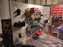
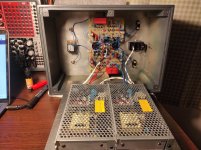
A couple of photos of the prototype:


I would appreciate any feedback.
Eugene
Also I decided to make an experiment and reduce output degeneration to the bare minimum just enough to make protection circuits work and use thermistor for quiescent current stabilisation.
Originally it was meant to have 20W of class A power but during prototyping I have reduced the bias to about 15 to lower the dissipation. Also it took multiple heating and cooling cycles to adjust the amount of thermal compensation. So it would be a good idea to use a some sort automatic biasing circuit.
A couple of photos of the prototype:
I would appreciate any feedback.
Eugene
Attachments

I've made a few minor changes to the layout and decided to make a small experiment. I made a "paper and epoxy" silkscreen. Yes, it's just a paper covered (and infused) with epoxy resin. The surface is not very uniform so curing under pressure would be helpful. The uncured resin partially dissolves the toner which led to a slightly fuzzy image.

Very interesting, is that a laser print?I made a "paper and epoxy" silkscreen.
Yes it is. And it looks much better than all my attempts to heat-transfer the tonerVery interesting, is that a laser print?
Just an offcut of FR4. But the resin doesn't have a strong surface tension so the paper lifts if too much resin has been squeezed out. So I'd try to use clamps next timeDid you use a paint roller to squeeze out the excess epoxy?
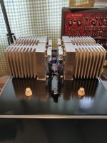
Here is the final look of the first working version. Not the most nicely looking build.


I utilised heatsinks designed for heavy duty stud mount diodes which I got for cheap. The case is made from MDF board, 2 stacked layers of 6mm. I just have a lot of leftovers from my pinhole camera project.
The thermistor based biasing circuit finally works fine but it was a huge pain in the butt to fine tune it to the point of just slightly positive temperature coefficient. An LPF based auto bias circuit would be a much better choice.
I'm a bit tired now but in the future I may redesign it with improved biasing circuit and lower number of resistor values. And draw a two-sided PCB for it.
Here is an FFT view from LTspice. It shows very little of high-order harmonics thanks to heavily linearised hybrid LTP. Both BJT-only and JFET-only versions showed (a bit) worse performance here.

In case someone wants to play with Spice I attached the self contained project archive
In case someone wants to play with Spice I attached the self contained project archive
Attachments
- Home
- Amplifiers
- Solid State
- Transconductance mode (bufferless) hybrid BJT/FET class A amplifier codenamed Cicada