Hi all,
I am trying to redesign/make a TPA3251 amplifier with good components.
Most of you must already know that the PFFB approach has better results for all parameters, than a standard configuration according to TI's "slaa778" document.
However,
There seems a problem occours when you use PFFB topology according to this document!
The total gain reduces to 12.75 dB (x4.34) in this case, which is fairly low !
You may say, "so drive it with a pre, or increase the front end stage's gain".
But according to TPA3251's datasheet, maximum input swing is limited to 7Vpp..
So if we apply 7Vpp = 2,48Vrms to inputs then the output power will be just 29W@4R, if you consider the total gain of amplifier.
And this is the limit value, you cannot reach the 2,48v level in any case.
..
So what do you think about that?
Isn't there any way to make a powerfull amplifier with PFFB topology?
Hi,
Did you use the circuit as per the Figure 2 in the PFFB application note ?
I would expect that the gain of the forward path is set in the TPA3251, and the PFFB is reducing the voltage at the input pin so as to reduce the closed loop gain to 12.75dB for the same input to the buffer opamp as per Figure 2.
The THD versus power graphs show that with the PFFB, the power levels greater than 29watts into 4ohms is possible.
Regards,
Shadders.
Last edited:
Yes I use figure 2.Hi,
Did you use the circuit as per the Figure 2 in the PFFB application note ?
I would expect that the gain of the forward path is set in the TPA3251, and the PFFB is reducing the voltage at the input pin so as to reduce the closed loop gain to 12.75dB for the same input to the buffer opamp as per Figure 2.
The THD versus power graphs show that with the PFFB, the power levels greater than 29watts into 4ohms is possible.
Regards,
Shadders.
TI says that the gain is12.75dBin that sheet. But as you mentioned; in the same sheet they show 100+w power levels at THD graphic (fig.70)..
However, TPA3251 datasheet says max swing level is 7v.. How its possible????
Thats confusing.
Hi,Yes I use figure 2.
TI says that the gain is12.75dBin that sheet. But as you mentioned; in the same sheet they show 100+w power levels at THD graphic (fig.70)..
However, TPA3251 datasheet says max swing level is 7v.. How its possible????
Thats confusing.
I have not modelled the PFFB, but it has to be applying negative feedback. That negative feedback is subtracting from the input signal from the opamp output in Figure 2.
The opmp buffer in Figure 2 is unity gain as per the values in Table 1 of the PFFB document. You could change the resistor R_op_fb (10kohm) to a higher value to achieve more gain - but check with TI forum that this will not cause any issues.
You could use a pre-amp as suggested.
If you apply a 7volt signal to the input of the unity gain opamp buffer, the voltage seen by the TPA3251 input pin is less than 7vots due to the PFFB.
I suppose TI should state the max voltage that can be applied to the input to make it more obvious what is happening.
Regards,
Shadders.

I already read the topic in TI's forum about that matter. But they did not mention anything about reaching 7v input levels. They just recommended to use a preamp stage.. And nothing about the max voltage..Hi,
I have not modelled the PFFB, but it has to be applying negative feedback. That negative feedback is subtracting from the input signal from the opamp output in Figure 2.
The opmp buffer in Figure 2 is unity gain as per the values in Table 1 of the PFFB document. You could change the resistor R_op_fb (10kohm) to a higher value to achieve more gain - but check with TI forum that this will not cause any issues.
You could use a pre-amp as suggested.
If you apply a 7volt signal to the input of the unity gain opamp buffer, the voltage seen by the TPA3251 input pin is less than 7vots due to the PFFB.
I suppose TI should state the max voltage that can be applied to the input to make it more obvious what is happening.
Regards,
Shadders.
Hi,I already read the topic in TI's forum about that matter. But they did not mention anything about reaching 7v input levels. They just recommended to use a preamp stage.. And nothing about the max voltage..
The gain of the TPA3251 IC is fixed at 20dB, and from the datasheet the input pin is inverting (page 7 of datasheet). The PFFB (post filter feedback) signal subtracts from the audio input signal, to reduce the actual voltage signal at the TPA3251 input pin.
The voltage required to achieve maximum power will be +/-2.474volts (rms) +7.2dB = +/-5.67volts (rms) (+/-8.01volts peak).
As long as the pre-amp has the capablity to output +/-8volts peak, then you will achieve the full output power of the TPA3251. Alternatively, you could increase the gain of the inverting input buffer by 2 should your source be unable to achieve the 8volts peak, but i would check with the TI forum to ensure that the change in buffer gain does not affect the PFFB.
Regards,
Shadders.
7Vpp is per channel. Since it's taking balance input, consider the total Vpp to be 14V for differential.
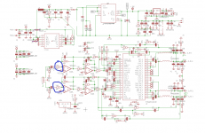
This is my application circuit (sorry for a bit "crowded" drawing..)
I'll change the input (R13&R18) resistors value to 4K7 etc..
Attachments
Last edited:
Hi,7Vpp is per channel. Since it's taking balance input, consider the total Vpp to be 14V for differential.
I would disagree with this. The datasheet for the TPA3251, page 22, Table 6, states each analogue input has a maximum peak of +/-3.9volts. As such, +3.9volts on input A, and -3.9volts on input B is a differential of 7.8volts.
Regards,
Shadders.
I agree with you. 🙂Hi,
I would disagree with this. The datasheet for the TPA3251, page 22, Table 6, states each analogue input has a maximum peak of +/-3.9volts. As such, +3.9volts on input A, and -3.9volts on input B is a differential of 7.8volts.
Regards,
Shadders.
So it's only 2.76Vrms differential input.
DXvideo.
The sch is wrong for input A and B. Out B is not connected.
Thanks a lot for warning.. I'll fix it.I agree with you. 🙂
So it's only 2.76Vrms differential input.
DXvideo.
The sch is wrong for input A and B. Out B is not connected.
Hi,I agree with you. 🙂
So it's only 2.76Vrms differential input.
I understand technically what you have written is correct, but the definition of the differential is confusing. A few years ago, at first glance i would have thought that the 14volts means +7volts A input and -7volts B input for a positive voltage swing, and vice versa for a negative voltage swing.
From a practical implementation approach, the 14volts definition would have confused me.
Regards,
Shadders.
Consider one half bridge, i.e. a single ended output.
Max output voltage is limited by power supply voltage.
With 36Vdc you can expect about 30Vpp at clipping.
Inverting input voltage is given by TPA3251 inverting gain, say 20dB.
Thus the inverting input voltage for output clipping is about 3Vpp.
Far below 7.8Vpp.
Always, fixed by the TPA3251 gain - no matter what PFFB network you use!
Accordingly In a full bridge 2 x 3Vpp inverting input voltage for 60Vpp output.
The PFFB network feeding input voltage certainly is higher - but this is not the point here.
Last edited:
hi, i also going to add pffb to non-pffb board. Did you found the solution? Do change value of R_in get good result?
- Home
- Amplifiers
- Class D
- TPA3251 PFFB Gain problem !