Hi,
I'm currently trying to wrap my head around Nelson's patent for the optobias (# 4752745) as I like the idea to add a sliding bias output stage to my current project amp.
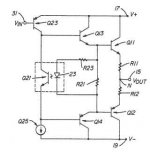
The concept is simple yet elegant (typical for Nelson) and works about as follows:
R21 provides a measure of the driver bias; its voltage drop is about 1.2V or larger (we're talking GaAs diode); if it's larger, R23 is necessary to reduce current through the diode 23.
The larger the current trough R21, the larger the current in diode D23; this diode drives the base of Q21 with a current transfer ratio of, say 5 (means the current through Q21 is 5 times the diode forward current). So more current through the diode yields more current in Q21.
So far so good; however how does that yield a larger VBE for the drivers?
There's a current source drawn - Q25 -, however that would reduce the collector-emitter voltage across Q21 if the current through Q21 increases - so does exactly the opposite of what one wants.
Unfortunately I couldn't find a single schematic with part values that includes optobias, so I hope somebody could enlighten me!
It's a pity that this patent is not as elaborate as the first smart bias patent (which even included 3 full amp schematics), it even mentions I1 and I2 which are not drawn at all...
Have fun, Hannes
I'm currently trying to wrap my head around Nelson's patent for the optobias (# 4752745) as I like the idea to add a sliding bias output stage to my current project amp.
The concept is simple yet elegant (typical for Nelson) and works about as follows:
R21 provides a measure of the driver bias; its voltage drop is about 1.2V or larger (we're talking GaAs diode); if it's larger, R23 is necessary to reduce current through the diode 23.
The larger the current trough R21, the larger the current in diode D23; this diode drives the base of Q21 with a current transfer ratio of, say 5 (means the current through Q21 is 5 times the diode forward current). So more current through the diode yields more current in Q21.
So far so good; however how does that yield a larger VBE for the drivers?
There's a current source drawn - Q25 -, however that would reduce the collector-emitter voltage across Q21 if the current through Q21 increases - so does exactly the opposite of what one wants.
Unfortunately I couldn't find a single schematic with part values that includes optobias, so I hope somebody could enlighten me!
It's a pity that this patent is not as elaborate as the first smart bias patent (which even included 3 full amp schematics), it even mentions I1 and I2 which are not drawn at all...
Have fun, Hannes