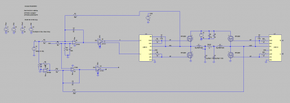
I'm experimenting with a three-level PWM class D design with GAN Fets for a school project. The current simulation uses the LM5113 driver which has no dead time control, however my final design will use PE29102 or the new LMG1210 (These drivers don't have LTspice models so the LM5113 will do for now).
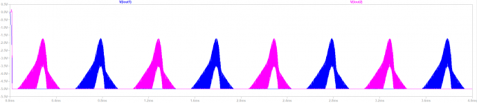
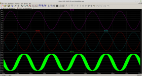
I'm running in to some problems with higher frequencies. The simulation shows sub 0.1% thd at 1kHz, 1.4V but as the frequency increases, the output attenuates.
E.g at 10kHz, Vout = 10V amplitude, at 15kHz, Vout = 3V amplitude etc.
Is it obvious to anyone what the cause of this is? I assume it has to do with the gain of the integrator or possibly the output filter but i'm not sure after a bunch of testing. I'll attach the spice files.
Attachments
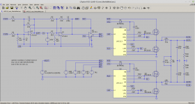
Given you have VCC and VCC-, try using VCC and VEE as the labels. It's more conventional, and your ICs can handle +/-5V forget about trying to use Vref to bias things. Make your triangle wave +/-2.5V. You have not supplied the high side drive supply, HB. It needs a diode. Check the LM5113 data sheet.
Your triangle swings 5V in 1.25uS dV/dT= 4E6V/S. Use 100pF capacitors in your integrators. To get 4E6V/S at the output you need to drive a current of 400uA. With your 30V bridge supply that makes the feedback resistors 75K... you don't want to overcook things so use your 100K ones. BTW, its called Slope Matching. Peak ramp of the error amplifier output should not exceed the triangle ramp. If it does things will try to switch at really high frequencies. Have a think about that one. You will notice that using the above the zero output error amplifier triangle will/should be half the amplitude of your reference triangle. Bandwidth works out to be Fs/PI.
Oh. My copmuter says your zip file is corrupt but that might be me running Linux.
Thanks for the advice, I've updated the schematic with your suggestions but the integrator output seems to saturate at -5V and attempt to follow the input for the top half of the signal. I'll attach the new files again, hopefully you can open them.
Attachments
Thanks for the advice, I've updated the schematic with your suggestions but the integrator output seems to saturate at -5V and attempt to follow the input for the top half of the signal. I'll attach the new files again, hopefully you can open them.
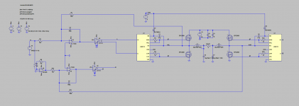
Oooops. Sorry. Too much alcohol. Something like the attached.
I've messed about with stuff. Bigger gate resistors on your driver ICs to tame cross-conduction and other bits. I guess the big one was using lower value resistors, bigger integrating capacitors, for the feedback.
You really need to think about the required bandwidth of the various amplifiers and input offset voltages and bias currents. If you don't then you end up with overall output offset voltages robbing you of available output and paying too much money.
Some other bits have changed. Mainly operating levels and also the output filter. Don't quote me on that one. It's a guess at 40KHz cut off for an 8R load.
Obviously I dicked about with things until they worked. You can have a poke about and do some sums to see if it might make sense. Bricks it at 20KHz... I was surprised.
Attachments
Oooops. Sorry. Too much alcohol. Something like the attached.
I've messed about with stuff. Bigger gate resistors on your driver ICs to tame cross-conduction and other bits. I guess the big one was using lower value resistors, bigger integrating capacitors, for the feedback.
You really need to think about the required bandwidth of the various amplifiers and input offset voltages and bias currents. If you don't then you end up with overall output offset voltages robbing you of available output and paying too much money.
Some other bits have changed. Mainly operating levels and also the output filter. Don't quote me on that one. It's a guess at 40KHz cut off for an 8R load.
Obviously I dicked about with things until they worked. You can have a poke about and do some sums to see if it might make sense. Bricks it at 20KHz... I was surprised.
Ah, thanks for that. I assumed a differential amplifier would be the best option with a single integrator. Is there any reason you have the resistor in series with the cap in the integrator?
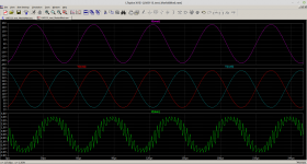
I tweaked some things and added three level modulation and it's running at less than 0.1% thd through the audio band.
Thanks for the advice about the opamps, I'll have a look into it.
U1 is the, main, integrator and differential amplifier combined. The resistors place the nominal 15V per leg output of the bridge down at about 2V within the supply range of U1. The capacitors convert the square waves to a triangle wave.
U2 lets you adjust the resulting triangle amplitude to match your clock triangle and set the input to output gain. You also get to add C5 increasing the low frequency gain. It is not the main integrator you just kind of get it for free but you have to worry about loop stability problems if you use it.
U2 lets you adjust the resulting triangle amplitude to match your clock triangle and set the input to output gain. You also get to add C5 increasing the low frequency gain. It is not the main integrator you just kind of get it for free but you have to worry about loop stability problems if you use it.
Do you think that replicating lowest performing circuits like triangle wave with newest hardest to manufacture transistors like GaN brings any progress? This is like sewing the future to the past.
Eva it's for school, so there's a huge element of learning and far less about advancing the state of the art.
Eva it's for school, so there's a huge element of learning and far less about advancing the state of the art.
Using expensive FETs together with obsolete principles is like teaching computer technolgies but only up to relays but with its housing being gold plated. Don't you think it would be much more useful to learn actual electronics of this time instead of something which won't be use anymore?
Not too sure. All we are doing is bolting latest tech power devices to latest tech level shifting power drivers. The old school control can be replaced at a later date if you want the latest flash bang. It's all experience.
Not too sure. All we are doing is bolting latest tech power devices to latest tech level shifting power drivers.
Latest tech? You do realize TI put specifically "Not Recommendedfor NewDesigns" into the datasheet? Why do you think would they do that on 'latest tech'? 🙄
The school project specifically mentioned modulation techniques of either PWM or PDM so the majority of my effort went into those designs. I found this website much later in the project timeline and didn't care to spend a significant amount of effort changing the design for new modulation techniques. I still may have time to consider other designs as the modulation stage can be chopped and changed relatively easily.
Could one of you elaborate on these new modulation techniques?
Could one of you elaborate on these new modulation techniques?
The first thing is, PDM or PPM poses a much lower strain on the power supply than PWM because it pulses more often than a PWM at the same clock frequency and therefore does not use that much current within a short time period. The result are much less losses and therefore heat, higher efficiency and much smaller parts dimensioning. That's why chips like the TDA8932 or TPA3118 can be used with minimal or no cooling or heat sink at power output values which were impossible with i.e. PWM amps with the same enviroment.
The second thing is probably more important (at least for HiFi enthusiasts), the much lower strain on the power supply results in a very good sound even with smaller, simpler and much cheaper power supplies.
Difference Between PAM, PWM, and PPM - Comparison of PWM and PAM
or search for other comparisons.
I've found this comparison for self oscillating amplifiers which seems really interesting: https://hal.archives-ouvertes.fr/hal-01103665/document. But he doesn't go into the calculations for the feedback phase components or coupling resistor etc.
Are there any good resources for designing these that you're aware of on this site or elsewhere?
Are there any good resources for designing these that you're aware of on this site or elsewhere?
..... That's why chips like the TDA8932 or TPA3118 can be used with minimal or no cooling or heat sink at power output values which were impossible with i.e. PWM amps with the same enviroment.......
TDA8932 and TPA3116/18 use PDM/PPM, not PWM?
Last edited:
TDA8932 and TPA3116/18 use PDM/PPM, not PWM?
They are self oscillating amplifieres which change the oscillating frequency/rate. Even if they both mention PWM in the datasheet, they are technically PSSO (Phase-Shift Self-Oscillating) or PPM (Pulse Position Modulation) amplifiers. The oscillator switching frequencies actually shift/re-position the pulses strategically. The high efficiency and very low heat dissipation of them can't be reached by traditional fixed frequency PWM amplifiers. NXP talks about PWM but gives a hint with mentioning it with a digital timing manager, TI speaks about 'advanced oscillator/PLL circuit employs multiple switching frequencies', both not going into detail any further, possibly using variants of the modulation methods.
Many thanks for the qualified explanation. That is the type of information they do not share with us.
Eva it's for school, so there's a huge element of learning and far less about advancing the state of the art.
School? What is being teached?
Did you know that the estimated ability to obtain Gallium from Earth, if all minor amounts from other minerals were reclaimed (as it does not happen on its own) are roughly 10 times current production?
Gallium - Wikipedia
There is not going to be any GaN semiconductor boom massively replacing silicon. Oh, wait a minute, maybe when countries start to fight for it. Nah...
Oh, but is someone stealing people's creativity with theories of boom materials? Nah...
- Status
- Not open for further replies.
- Home
- Amplifiers
- Class D
- Three Level PWM amplifier