What are your thoughts on this amp? See attached schematic. I recently came into possession of this amp, a Classe 70. Since they're out of business and the schematic is readily available, I'm curious as to what you think of the design, which they apparently used on every amplifier basic form and simply scaled it accordingly
The schematic is towards the end of the document ...
PS, sorry for the wrong attachment in the forum posting down below ...
The schematic is towards the end of the document ...
PS, sorry for the wrong attachment in the forum posting down below ...
Attachments
Last edited:
It must be something wrong in the schematic: R110 connected to the minus supply has the consequence that Q107 fully on makes the circuit not to work at all.
I'm not seeing the issue with R110/Q107, there's a voltage divider between D101+D102 & R108||R109. But without going through the numbers it does look like Q106 & Q107 are swapped - Q107 should be the MJE350 (and on a heatsink; this could be a documentation error in the svc manual, perhaps intentional). Among other things, Q102/Q104 base voltages appear to be ill defined (looks like it depends on the beta of the devices...). Interesting that they used output devices as driver transistors, maybe it made their assembly easier? Overall this design looks like one that is optimized to get the max performance out of the minimum number of components - other than the cascodes it has barely more parts than IIRC a Lin topology.
Yeah. Something is fishy around Q107/R110.
Q106 is a current mirror. It uses the voltage developed across D101, D102 as its reference. As does Q105. It looks like Q107 should have been a cascode. And it might be if it somehow, miraculously develops enough base current to set up a good bias point across R110. This bias point will depend entirely on the characteristics of Q107, so if the amp is built as per the schematic, it won't be a very reliable or reproducible design. It makes me wonder if the schematic is incorrect and R110 should have connected elsewhere.
I would rather bias Q107 in a way similar to the bias of Q109.
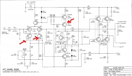
Some of the protection circuitry (page 14) could be worth keeping, though.
Tom
Q106 is a current mirror. It uses the voltage developed across D101, D102 as its reference. As does Q105. It looks like Q107 should have been a cascode. And it might be if it somehow, miraculously develops enough base current to set up a good bias point across R110. This bias point will depend entirely on the characteristics of Q107, so if the amp is built as per the schematic, it won't be a very reliable or reproducible design. It makes me wonder if the schematic is incorrect and R110 should have connected elsewhere.
I would rather bias Q107 in a way similar to the bias of Q109.
Some of the protection circuitry (page 14) could be worth keeping, though.
Tom
Could be a schematic drafting error .. or maybe the unusually high value of R110 is nevertheless supposed to keep Q107 saturated until, say, about the lower 1/4 of output swing. At 46V (approximate, quiescent) across 274k is ~170uA. That's enough for a typical MPSA56 to conduct 15 to 22mA, keeping it saturated over most of the output range.
Maybe the designer believed adding Q107 improved the *symmetry*, since the VAS is cascode .. ?
Sure seems like part-to-part variability of Q107 would give Outgoing QC/QA guys some bad nightmares.
Then there's the issue of the MPSA06/56 being 80V parts, with ~90V of rails ..
Cheers
edit: Sorry if this is redundant -- been typing since the post #3 slot was next.😱
Last edited:
This might be the model amplifier previously discussed here (it was this brand either way) where the two transistors in a cascode were found to be obviously swapped on the schematic... only for the real thing to be checked and turning out to be built exactly like that! Oops. 😱 Heaven knows how they even survived for all these years with an obvious screwup like that... it has to be a testament to the overvoltage handling of these MPSA transistors.
This might be the model amplifier previously discussed here (it was this brand either way) where the two transistors in a cascode were found to be obviously swapped on the schematic... only for the real thing to be checked and turning out to be built exactly like that! Oops. 😱 Heaven knows how they even survived for all these years with an obvious screwup like that... it has to be a testament to the overvoltage handling of these MPSA transistors.
Can you try to find that post on the Classe amp with the issue and email me the link? I searched, no luck
I just confirmed that Q106 and Q107 on the circuit board are exactly as specified on the schematic, ditto Q206 and Q207 for the other channel. Looks like a major screw up by Classe.
Can someone model this circuit for me and tell me the stability, etc.???
Can someone model this circuit for me and tell me the stability, etc.???
It must be something wrong in the schematic: R110 connected to the minus supply has the consequence that Q107 fully on makes the circuit not to work at all.
No that is not an error - the post shows only page 12 of a 15 page document. When you scroll to page 11 you will see that.
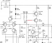

Maybe resistor should move like this, giving ratio of ~ 25:275
Similar in concept to what i used in this other example of the cascoded input side.
That's reasonable, and since there are more errors: Is this deliberate from Classe Audio?
I am referring to the left channel circuitry on page 11, I don't see another schematic.
The labels on the schematic shown on page 12 show the connections to the non-inverting input and the inverting input.
The image on page 11 shows in block form the buffer op.amps and the switching arrangement for balanced - mainly seen in professsional use with long cable runs and in high end audio. Unbalanced feed is the normal switch setting for domestic product.
There is more detail on this in page 13 which shows one op.amp configured in non-inverting mode and the other in inverting mode.
Had this switching arrangement not been adopted R107 would connect to earth.
Based on .65V across R103, Q102 and Q104 bases would sit around 16V above the negative rail with beta of 100, 32V with beta of 50. Should work.
Maybe the designer believed adding Q107 improved the *symmetry*, since the VAS is cascode .. ?
Well, it will make the clipping more symmetrical, won't it?
Based on .65V across R103, Q102 and Q104 bases would sit around 16V above the negative rail with beta of 100, 32V with beta of 50. Should work.
Yes, you are right.
Q107 does look like it's operating in some degree of saturation most of the time...Yes, you are right.
- Home
- Amplifiers
- Solid State
- Thoughts on this schematic?