Hello,
I played a bit with LTSpice here, according to a circuit diagram I found in my documents, I don't know which device it came from, I just found this sheet, hand-drawn, and found it interesting.
I think the performance of the amp is not that bad, but I'd be interested in some feedback from you guys on what can be improved before I try to make a PCB design for it.
Thanks in advance!
Lukas
Attachments
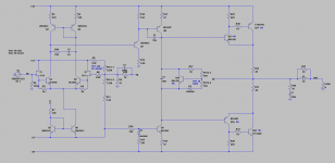
Current sources
Current mirrors?
Lots of Szlikais
I think Q₉ is being base driven to a virtual ground.
So then what's the point of R₁₅ R₁₆ D₃ and of course R₁₁
⋅-⋅-⋅ Just saying, ⋅-⋅-⋅
⋅-=≡ GoatGuy ✓ ≡=-⋅
Current mirrors?
Lots of Szlikais
I think Q₉ is being base driven to a virtual ground.
So then what's the point of R₁₅ R₁₆ D₃ and of course R₁₁
⋅-⋅-⋅ Just saying, ⋅-⋅-⋅
⋅-=≡ GoatGuy ✓ ≡=-⋅
I'd be interested in some feedback from you guys on what can be improved before I try to make a PCB design for it.
Hi, Lukas!
Not bad!
But it can be a way better.
1. Input.
Why too complicated?
Now JFETs acts as a buffer, leave them alone, they're great themselves. Only this will safe you from dedicated +-15V supply.
Current mirror Q3Q4, just add third transistor to make a much more precise Wilson mirror.
Current source Q5Q6, just rewire them to allow Q5 track voltage at the added Q6's emitter resistance or make cascoded current source, this will improve your current source stability against common mode error through much wider common mode range.
C3R24 - perfect! High-impedance point freq correction are very easy and very potent.
2. Voltage amification (aka current-to-voltage) stage.
Q7 as a buffer - excellent!
C1 as a Miller correction are ugly, be sophisticated, go to TMC, TPC or OITPC correction. 33p will kill your's amp sounding at high freqs, this will significantly lower dominant pole and drop feedback depth where it's very needed. With them in place you'll achieve classical harsh transistor sounding anyway.
BD140BD139 are driver transistors and not good to be last VAS devices, too high reverse transfer capacitance. Try to find KSC3503KSA1381 devices for this point.
Lower current source are wired strangely, just use the same block as for input stage.
3. Output.
Bad decision. First devices have too large input capacitance to be coupled to VAS output straightly.
Such an OPS will have huge input resistance variance over output current and because of this will provide huge VAS load change. All of this will hardly put your's amp to be unstable or bad sounding. Use a well-known triple of emitter followers or bipolar+lateral MOSFET pair of followers.
4. Common questions.
It's bad to use common supply for low-current and high-current parts of an amp. You anyway have limited power supple regection ratio and because of this it's better to decouple them. Also output stage usually better to be driven to the power rails and because of this there are usually dedicated higher supply rails for low-current circuitry up to output driver transistors.
Rewire overall amp topology to be inverting, this topology are free from common mode error, this usually underestimated.
\Commooooo I followed you here from a closed post about a Technics SU-V2 phono issue with SVITA7322 chip. I have the same issue and I was wondering if you could share a picture of what you ended up doing as I'm a layman with soldering skills and I believe I can get the chip you used but I wanted to make sure I dont make the problem worse
Last edited by a moderator: