This post started a little experiment.
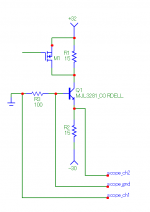
Since most transistors parameters depend on temperature, the instantaneous junction temperature would be an interesting thing to know. It isn't measurable in-circuit while an amplifier is working, but Vbe provides access to it if the transistor passes a constant current. So, here we go:

Here's the procedure:
- The MOSFET is left open for now
- Knobs on the bench power supply are turned until the transistor under test has a suitable current (2 Amps here) and a low Vce (2 Volts). The BJT should not be in saturation. Here, it dissipates about 5 watts at idle.
- Since the supply is floating, the scope GND can be connected to a convenient place. One channel measures Vbe, the other hFe, via the base resistor and the known collector current.
- Wait a bit for the temperature to stabilize.
- Turn on MOSFET, record waveforms, turn off MOSFET.
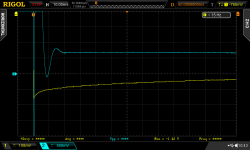
This setup is quite simple and ghetto, however there are two interesting traps that I tried to avoid:
1) The bench PSU outputs a quasi constant current. Therefore I am not testing its transient response.
2) The opamps inside the scope inputs must not clip! This setup allows both inputs to swing very little during the experiment. It would be a very bad idea to drive the BJT from its base...
The MOSFET is switched on and off using a manual switch. It debounces it and makes switching soft and slow. This is essential to avoid a small spike, which is enough to make the opamp at the input of the scope clip. This would be the result:

The blue trace measures a signal which doesn't exist. It is simply the input opamp coming out of clipping and having trouble sorting out the fact that its input stage has a warm side and a cold side. It is called a thermal tail. This opamp, which has at least 300MHz bandwidth, takes more than 20ms to settle. Never trust your scope if the trace clips!...
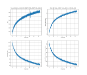
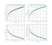
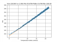
And now, with a bit of "export trace to USB key" and some python code, we get the last three graphs. This time I used Vbe under constant current as a thermometer, so the temperature readings should be accurate.
We see how Tj evolves through time as this transistor is exposed to a constant 55W dissipation. To be continued...
Since most transistors parameters depend on temperature, the instantaneous junction temperature would be an interesting thing to know. It isn't measurable in-circuit while an amplifier is working, but Vbe provides access to it if the transistor passes a constant current. So, here we go:
Here's the procedure:
- The MOSFET is left open for now
- Knobs on the bench power supply are turned until the transistor under test has a suitable current (2 Amps here) and a low Vce (2 Volts). The BJT should not be in saturation. Here, it dissipates about 5 watts at idle.
- Since the supply is floating, the scope GND can be connected to a convenient place. One channel measures Vbe, the other hFe, via the base resistor and the known collector current.
- Wait a bit for the temperature to stabilize.
- Turn on MOSFET, record waveforms, turn off MOSFET.
This setup is quite simple and ghetto, however there are two interesting traps that I tried to avoid:
1) The bench PSU outputs a quasi constant current. Therefore I am not testing its transient response.
2) The opamps inside the scope inputs must not clip! This setup allows both inputs to swing very little during the experiment. It would be a very bad idea to drive the BJT from its base...
The MOSFET is switched on and off using a manual switch. It debounces it and makes switching soft and slow. This is essential to avoid a small spike, which is enough to make the opamp at the input of the scope clip. This would be the result:
The blue trace measures a signal which doesn't exist. It is simply the input opamp coming out of clipping and having trouble sorting out the fact that its input stage has a warm side and a cold side. It is called a thermal tail. This opamp, which has at least 300MHz bandwidth, takes more than 20ms to settle. Never trust your scope if the trace clips!...
And now, with a bit of "export trace to USB key" and some python code, we get the last three graphs. This time I used Vbe under constant current as a thermometer, so the temperature readings should be accurate.
We see how Tj evolves through time as this transistor is exposed to a constant 55W dissipation. To be continued...
Attachments
-
 test-setup.png3.1 KB · Views: 735
 -
 scope thermal settling.png9.6 KB · Views: 690
 -
 Vce=28.00V Ic=1.95A Pd=55.87W Pidle=5.07W Rb=100.00 0.png105.7 KB · Views: 282
 -
 Vce=28.00V Ic=1.95A Pd=55.87W Pidle=5.07W Rb=100.00 1.png102.1 KB · Views: 124
 -
 Vce=28.00V Ic=1.95A Pd=55.87W Pidle=5.07W Rb=100.00 2.png96.8 KB · Views: 113
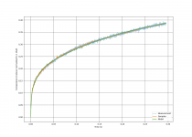
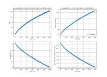
Now, let's plot hFe versus temperature. The relationship isn't linear, rather exponential from a temperature in °K, but as long as it isn't hot enough to blow it up, a linear approximation will do just fine.
Quick parameter fit:
Note: "Temp" is the temperature variation between the time the MOSFET was switched on and the current time. I have no idea of the absolute temperature, probably 40-50°C... but it doesn't matter a lot. The point to remember here is that this transistor gains 0.5% hFe per celsius.
Now, on to thermal modeling...
Quick parameter fit:
Code:
MJL1302 : hFe = 140.853154 + 0.721393*TempNote: "Temp" is the temperature variation between the time the MOSFET was switched on and the current time. I have no idea of the absolute temperature, probably 40-50°C... but it doesn't matter a lot. The point to remember here is that this transistor gains 0.5% hFe per celsius.
Now, on to thermal modeling...
Attachments
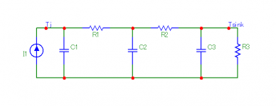
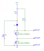
Now, wouldn't it be nice if we could have a model like this:

- Current source on the left represents dissipated power in transistor
- Tj is expressed in Volts
- Tsink (at the other end) would be the temperature of the transistor back, which touches the heatsink.
I have no interest in accurately modelling the heat sink, as it reacts very slowly. This model only tells what happens inside the transistor during about one second, which is a time scale compatible with analyzing safe operating area, fast thermal runaway and bias shifts.
Now, about 20 lines of code later... The idea is to compute the impedance, then the step response with FFT, and use a canned optimization function from scipy. Half a page of code... this software package is amazing.
This gives the graph on the right.
To use this model, R3 should be adjusted so that R1+R2+R3 correspond to the total thermal resistance between junction and free air. It will not simulate the heat sink thermal mass, but it will allow to see if a few pulses of high power signal push the transistor out of its SOA, which is always nice to know.
- Current source on the left represents dissipated power in transistor
- Tj is expressed in Volts
- Tsink (at the other end) would be the temperature of the transistor back, which touches the heatsink.
I have no interest in accurately modelling the heat sink, as it reacts very slowly. This model only tells what happens inside the transistor during about one second, which is a time scale compatible with analyzing safe operating area, fast thermal runaway and bias shifts.
Now, about 20 lines of code later... The idea is to compute the impedance, then the step response with FFT, and use a canned optimization function from scipy. Half a page of code... this software package is amazing.
Code:
MJL1302
C1 = 0.0102021555832
R1 = 0.0997718886805
C2 = 0.12149333978
R2 = 0.104840396696
C3 = 1.00087678259
R3 = 0.191614159075
This gives the graph on the right.
To use this model, R3 should be adjusted so that R1+R2+R3 correspond to the total thermal resistance between junction and free air. It will not simulate the heat sink thermal mass, but it will allow to see if a few pulses of high power signal push the transistor out of its SOA, which is always nice to know.
Attachments
I just tested the complementary NPN, MJL3281.
Now, something very interesting. While the sum of R1+R2+R3 in both models are almost identical, which means the package thermal resistances should be matched, transient behavior is very different. The PNP's temperature rise is much sharper, as it gains more than 5°C in only a few milliseconds, whereas the NPN behaves like it has a lot more thermal mass.
This is quite weird...
Code:
MJL3281
hFe = 115.567551 + 0.410725*Temp ==> 3.6% per °C

C1 = 1.17733316782
R1 = 0.0333437172786
C2 = 1.16526420761
R2 = 0.045204225319
C3 = 1.89219473491
R3 = 0.322956043959
Now, something very interesting. While the sum of R1+R2+R3 in both models are almost identical, which means the package thermal resistances should be matched, transient behavior is very different. The PNP's temperature rise is much sharper, as it gains more than 5°C in only a few milliseconds, whereas the NPN behaves like it has a lot more thermal mass.
This is quite weird...
Attachments
...Quick parameter fit:
Code:MJL1302 : hFe = 140.853154 + 0.721393*Temp
... 0.5% hFe per celsius.
I just tested the complementary NPN, MJL3281.
Code:MJL3281 hFe = 115.567551 + 0.410725*Temp ==> 3.6% per °C
Very nice to see actual data, not just subjective claims.
But looks like a decimal place is out?
Best wishes
David
Oops, yes, I seem to have nudged a decimal place.
I can't edit my post? Weird.
The difference between NPN and PNP is weird. I'll add a less "ghetto" test jig to my next batch of pcbs to investigate this...
I can't edit my post? Weird.
The difference between NPN and PNP is weird. I'll add a less "ghetto" test jig to my next batch of pcbs to investigate this...
Hi, the difference in thermal capacity between NPN and PNP might be due to the fact, that a NPN transistor really is a PNPNP transistor, as emitter and collector leads are metallic, hence positively charged. PNP is electrically faster than NPN, so it seems natural to be thermically faster, too.
I did another experiment to double check. This time, both NPN and PNP are wired as diodes, and they are wired in series to ensure the same current goes through both.

They are biased at a current of 0.6 A via a resistor to V+.
When the MOSFET opens, the current going through the 15R resistor goes through the diode, then the BJTs instead of going to GND.
Again this is to ensure I don't measure the power supply.
I realized I had missed a detail in the last setup: the scope did in fact clip, and I got bitten. I had set it in high-resolution mode, which time-averages samples to get more bits, so the smoothing effect hid a tiny inductive spike produced as the MOSFET switched.
I took care of it... and as a result, both PNP and NPN now have identical thermal behavior in the first milliseconds. This is their Vbe (two tests shown) as the high current is switched on:

I see no reason to doubt the hFe temperature coefficient between NPN and PNP, though. Only the thermal impedance measurement was affected.
So, this measurement was more complicated than expected, and this is related to how a power pulse is induced in the transistor.
- Changing Vce from 2 to 30V (as previously) requires a large spike in base current due to Miller effect. Measuring hFe right after this requires attention.
- Changing the current creates a step in Vbe. In order to accurately measure this, either an ADC with lots of bits is needed, or a proper limiting amplifier before the scope (without clipping effects on settling time)...
For some reason I can't edit my previous posts to correct...
They are biased at a current of 0.6 A via a resistor to V+.
When the MOSFET opens, the current going through the 15R resistor goes through the diode, then the BJTs instead of going to GND.
Again this is to ensure I don't measure the power supply.
I realized I had missed a detail in the last setup: the scope did in fact clip, and I got bitten. I had set it in high-resolution mode, which time-averages samples to get more bits, so the smoothing effect hid a tiny inductive spike produced as the MOSFET switched.
I took care of it... and as a result, both PNP and NPN now have identical thermal behavior in the first milliseconds. This is their Vbe (two tests shown) as the high current is switched on:
I see no reason to doubt the hFe temperature coefficient between NPN and PNP, though. Only the thermal impedance measurement was affected.
So, this measurement was more complicated than expected, and this is related to how a power pulse is induced in the transistor.
- Changing Vce from 2 to 30V (as previously) requires a large spike in base current due to Miller effect. Measuring hFe right after this requires attention.
- Changing the current creates a step in Vbe. In order to accurately measure this, either an ADC with lots of bits is needed, or a proper limiting amplifier before the scope (without clipping effects on settling time)...
For some reason I can't edit my previous posts to correct...
Attachments
Last edited:
Dear Peufeu,
I am glad I found this thread.
Did you continue further with your experimentation?
BTW, please take a look at my humble efforts based on your work and recommendations:
The AMNESIS amp: a good amplifier, like a gentleman, has no memory.
Amicalement votre,
M.
I am glad I found this thread.
Did you continue further with your experimentation?
BTW, please take a look at my humble efforts based on your work and recommendations:
The AMNESIS amp: a good amplifier, like a gentleman, has no memory.
Amicalement votre,
M.
- Status
- Not open for further replies.
- Home
- Amplifiers
- Solid State
- Thermal modeling of transistors