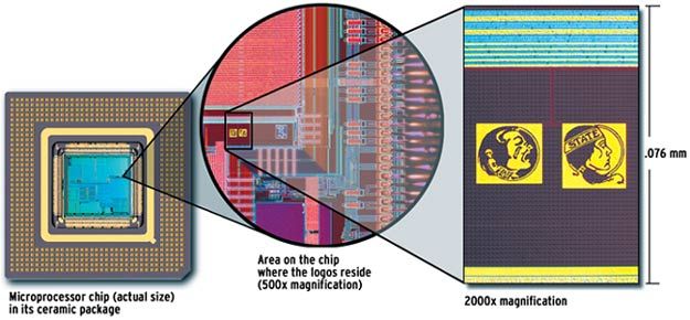
CHIP ART
Chip art, also known as silicon art, chip graffiti or silicon doodling, refers to microscopic artwork built into integrated circuits, also called chips or ICs. Since ICs are printed by photolithography, not constructed a component at a time, there is no additional cost to include features in otherwise unused space on the chip. Designers have used this freedom to put all sorts of artwork on the chips themselves, from designers' simple initials to rather complex drawings. Given the small size of chips, these figures cannot be seen without a microscope. Chip graffiti is sometimes called the hardware version of software easter eggs.
Prior to 1984, these doodles also served a practical purpose. If a competitor produced a similar chip, and examination showed it contained the same doodles, then this was strong evidence that the design was copied (a copyright violation) and not independently derived. A 1984 revision of the US copyright law (the Semiconductor Chip Protection Act of 1984) made all chip masks automatically copyrighted, with exclusive rights to the creator, and similar rules apply in most other countries that manufacture ICs. Since an exact copy is now automatically a copyright violation, the doodles serve no useful purpose.
Creating chip art
Integrated Circuits are constructed from multiple layers of material, typically silicon, silicon dioxide (glass), and aluminum. The composition and thickness of these layers give them their distinctive color and appearance. These elements created an irresistible palette for IC design and layout engineers.
The creative process involved in the design of these chips, a strong sense of pride in their work, and an artistic temperament combined compels people to want to mark their work as their own. It is very common to find initials, or groups of initials on chips. This is the design engineer's way of "signing" his or her work.
Often this creative artist's instinct extends to the inclusion of small pictures or icons. These may be images of significance to the designers, comments related to the chip's function, inside jokes, or even satirical references. Because of the difficulty in verifying their existence, chip art has also been the subject of online hoaxes (e.g. the never-seen "bill sux" comment on a Pentium chip—the reputed "photo" showing the inscription is a hoax[1]).
The mass production of these works of art as parasites on the body of a commercial IC goes unnoticed by most observers and is discouraged by semiconductor corporations, primarily from the fear that the presence of the artwork (which is clearly unneeded) will interfere with some necessary function in the chip or design flow.[2]
Some laboratories have started collaborating with artists or directly producing books and exhibits with the micrographs of these chips. Such is the case of Harvard chemist George Whitesides, who collaborated with pioneer photographer Felice Frankel to publish On the Surface of Things, a highly praised photography book on experiments from (mostly) the Whitesides lab. Also, the laboratory of Albert Folch (who, perhaps not coincidentally, works in BioMEMS, the same field as George Whitesides) at the University of Washington's Bioengineering Dept. has a highly popular online gallery with more than 1,700 free BioMEMS-related chip art micrographs [3] and has already produced three art exhibits in the Seattle area, with online sales.[4]
source :
http://en.wikipedia.org/wiki/Chip_art
The Secret Art Of Chip Graffiti - IEEE Spectrum
Silicon Art Library
video is on Ripley's Believe It or Not! Season 1 Episode 20
IS THERE ANY GRAFFITI INSIDE A LM1875?? 😀
Last edited:
Yea, there used to be a lot of that in the 70s and 80s. I remember Kilroy on an eeprom (1702A?).
NEC(?) caught a clone back in the 80s because the cloners didn't delete the small artwork from their top layer metalization mask.
NEC(?) caught a clone back in the 80s because the cloners didn't delete the small artwork from their top layer metalization mask.
I worked in a lab that designed and laid out IC chips. I have seen the layout guy put the UF Gators logo in 1st metal (visible with a good microscope) on several of our test chips (non production runs). Most productions chips have "tiling" over the surface on several metal layers to create uniform metal density for proper chemical etching during wafer processing. This makes images rather hard to find.
I have heard several versions of the "Bill Sux" story, and two ex Mot engineers DID get fired from Intel for putting something in a chip. Several of our designers knew one of the guys that lost his job. He would not talk about it. The reference quoted stated that the original article with the "Bill Sux" picture ran in the NY Times. I don't know about that paper, but it DID run in the EE Times (Electronic Engineering Times) trade publication. We cracked open several Pentium chips of the correct vintage and looked over them on our wafer probe station scope, but didn't find anything. I agree that the image shown in the EE times article is a fake, since you wouldn't put via holes in an image. There is no corresponding metal on the 2nd metal layer. Did it really happen? I don't know but I have seen some rather weird things in production equipment, and parts. Ours, and others.
I have heard several versions of the "Bill Sux" story, and two ex Mot engineers DID get fired from Intel for putting something in a chip. Several of our designers knew one of the guys that lost his job. He would not talk about it. The reference quoted stated that the original article with the "Bill Sux" picture ran in the NY Times. I don't know about that paper, but it DID run in the EE Times (Electronic Engineering Times) trade publication. We cracked open several Pentium chips of the correct vintage and looked over them on our wafer probe station scope, but didn't find anything. I agree that the image shown in the EE times article is a fake, since you wouldn't put via holes in an image. There is no corresponding metal on the 2nd metal layer. Did it really happen? I don't know but I have seen some rather weird things in production equipment, and parts. Ours, and others.
The second paragraph in post #1 confuses me. Maybe I'm just dense, but maybe not.
I can't recall the company name from the late-'90s, but they were fond of marine life chip images, including dolphins, octopuses, seahorses, etc. When looking at an IC at 2000x, they are cool to find.
I can't recall the company name from the late-'90s, but they were fond of marine life chip images, including dolphins, octopuses, seahorses, etc. When looking at an IC at 2000x, they are cool to find.
^@sofaspud yes I agree, the last sentence doesn't make sense. I would have thought that they served a very useful purpose in that it made it extremely easy to spot an "exact copy"!
Tony.
Tony.
- Status
- Not open for further replies.