Hello everybody
I'm not an expert but learned a lot reading this site. Thanks for that. This personal journey started some time ago, when I decided to build a DAC based on the TDA1541A
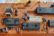
The first step was buying some old and malfunctioning CD player for a few bucks only to desolder and get the chip (photo attached).
Second step was to buy a JLSounds i2s over USB pcb v. 3, with the recommended mute card, then the rest of the components and a cheap enclosure.
Started easy but then I decided not to use a third party pcb but to solder point to point. Then added something new, a relay based volume control, just not to need any pre (passive or whatsoever) and to have all in only single box. Afterwards I decided to build the analog part without opamps, but with the simple FET-MOSFET as designed by Dietmar W. Gerhold (the "infamous" fetishizator V2.2) you can find on the web, and to use a simple but special non inductive resistor polarized at 0 Volts as the I/V converter. This last aspect also is not of mine but taken from this site threads. Thanks again for a lot of valuable information.
The only modifications to the fetishizator V.2.2 from Dietmar W. Gerhold were:
Reaching +/- 5V from a transformer with secondary rated +/-15V constrained me to use CRC with big resistors not to overload the LM3x7 chips, even with heatsink. This was a decision made and that's the reason I'm protecting some caps with a little cardboard piece (a hot 4 watts resistor nearby don't pleases me, even with 105 degrees caps).
The results:
After changing the fet source resistor to 330R during "commissioning" things started going very well. The sound is very very clear. This analog output can drive even headphones directly. My impressions are absolutely subjective. I'm driving an Aleph 30 clone with this and the sound is spectacular, specially in the highs, very clear and transparent. Hopefully this amp is not suffering from the ultrasonic load.
The only thing that can be annoying is the click of the relay based volume control, but as it only clicks when adjusting the output volume (the relay sound) this is something very bearable.
For the rest the sound is really amazing.
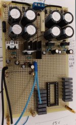
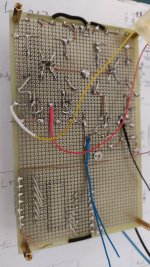
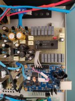
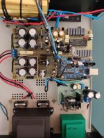
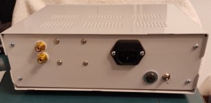
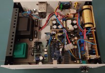
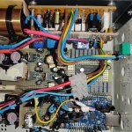
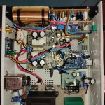
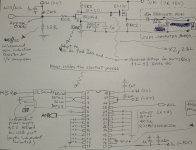
Some pictures of the journey, including one of my sketch sheets (not very good writing or designing things, excuse me for that). In the pictures from above the short description is: main boards are soldered point to point using the same components legs were possible. Only one ground wire without loops of any kind. At left the transformers. At right the two obbligato capacitors and the relay volume board. At the end, beside the output RCA connectors is the mute board (and the coils). The JLSounds card is inserted as a kind of daughterboard on top of the main pcb. The socket for the TDA1541A was presented but finally not used, and the cap legs are soldered directly to the TDA legs without any bridge.
Many thanks
I'm not an expert but learned a lot reading this site. Thanks for that. This personal journey started some time ago, when I decided to build a DAC based on the TDA1541A
The first step was buying some old and malfunctioning CD player for a few bucks only to desolder and get the chip (photo attached).
Second step was to buy a JLSounds i2s over USB pcb v. 3, with the recommended mute card, then the rest of the components and a cheap enclosure.
Started easy but then I decided not to use a third party pcb but to solder point to point. Then added something new, a relay based volume control, just not to need any pre (passive or whatsoever) and to have all in only single box. Afterwards I decided to build the analog part without opamps, but with the simple FET-MOSFET as designed by Dietmar W. Gerhold (the "infamous" fetishizator V2.2) you can find on the web, and to use a simple but special non inductive resistor polarized at 0 Volts as the I/V converter. This last aspect also is not of mine but taken from this site threads. Thanks again for a lot of valuable information.
The only modifications to the fetishizator V.2.2 from Dietmar W. Gerhold were:
- FET BF245A source resistor reduced to 330R to get the proper drain voltage to let it swing, something between 11 and 12 Volts (my FET happens to have a very particular Vgs)
- V+ set at 18 V
- 10 uF OBBLIGATO GOLD output capacitor and afterwards a 32R in series to have something to tame the "click" of the mute board when it shorts the AC output. With this it's 100% silent.
- added after the mute board (not because I'm sure it will filter something, but because it's better to have something than nothing) a very little air wound inductance hand made and measured to be 0.25 uH. This can make laugh but please stay put... 😉
Reaching +/- 5V from a transformer with secondary rated +/-15V constrained me to use CRC with big resistors not to overload the LM3x7 chips, even with heatsink. This was a decision made and that's the reason I'm protecting some caps with a little cardboard piece (a hot 4 watts resistor nearby don't pleases me, even with 105 degrees caps).
The results:
After changing the fet source resistor to 330R during "commissioning" things started going very well. The sound is very very clear. This analog output can drive even headphones directly. My impressions are absolutely subjective. I'm driving an Aleph 30 clone with this and the sound is spectacular, specially in the highs, very clear and transparent. Hopefully this amp is not suffering from the ultrasonic load.
The only thing that can be annoying is the click of the relay based volume control, but as it only clicks when adjusting the output volume (the relay sound) this is something very bearable.
For the rest the sound is really amazing.
Some pictures of the journey, including one of my sketch sheets (not very good writing or designing things, excuse me for that). In the pictures from above the short description is: main boards are soldered point to point using the same components legs were possible. Only one ground wire without loops of any kind. At left the transformers. At right the two obbligato capacitors and the relay volume board. At the end, beside the output RCA connectors is the mute board (and the coils). The JLSounds card is inserted as a kind of daughterboard on top of the main pcb. The socket for the TDA1541A was presented but finally not used, and the cap legs are soldered directly to the TDA legs without any bridge.
Many thanks
Attachments
-
 00 TDA1541A to desolder.jpg366 KB · Views: 285
 -
 01 TDA1541A First Presentation but not used.jpeg404.5 KB · Views: 178
 -
 02 TDA1541A First Steps.jpeg362.3 KB · Views: 182
 -
 03 TDA1541A First Tests.jpg527.3 KB · Views: 185
 -
 04TDA1541A First Tests 2.jpg496.4 KB · Views: 181
 -
 05 TDA1541A back.jpg181.5 KB · Views: 176
 -
 06 TDA1541A overall finished.jpg457.4 KB · Views: 165
 -
 07 TDA1541A finished 1.jpg792 KB · Views: 189
 -
 08 TDA1541A finished 2.jpg797.8 KB · Views: 191
 -
 09 TDA1541A finished 3.jpg621.1 KB · Views: 262
 -
 10 TDA1541A sketch Analog Part.jpg319.5 KB · Views: 268
Last edited:

Nice job, @jdamico . Some ideas for improvement:
You could try the Grundig DEM clock solution.
You could replace the 2.4k bias resistor at the DAC output with a jFET, set as a 2.0 mA current source, operated from +18 V.
Some attenuating resistors could be added in series with the three input signals of the DAC.
A heatsink could be attached on top of the DAC chip.