Hi
Everybody, I'm working on a Input and also Driver stage on a new Design for a Class A Amplifier.
The Point is this input is already build and it is running almost perfect.
Now nothing seems to be perfect,sometimes. as you will see..
I'm trying to increase the upper Frequency range of that Stage. This consists of 3 Transistors. It can be two as well, but if I use only two then I lose gain.
If I use three then Bandwidth will not Exceed 100Khz much. And output of Square Wave and also Sine wave will be Distorted, up to 1% comparing to 1Khz. The Circuit I have uploaded before already but I will upload it again, when I have Commented what has happen last night, in the circuit.
Now, this amplifier again with Output connected is build and it runs, but for my understanding there could be more. and has been tested already, and it sounds great, but I'm not finished with it yet.
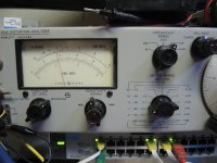
Last night while testing and preparing the PCB, By accident, I reversed somehow the BASE and EMITTER Pins, of the first Drive Transistor. Put on my desk, plugged in my Test Equipment and tested just the output of the second Drive Transistor. This I tested OPEN LOOP, so none Negative Feedback as well Output Transistors weren't connected yet, and applied Power.
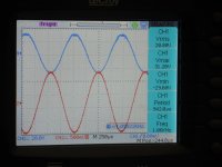
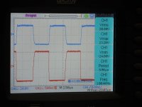
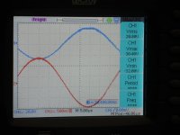
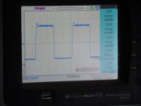
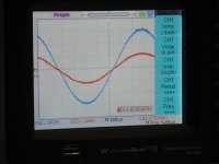
At that Time, this was last night, I didn't knew that I Reversed that Transistor, and started with 1KHz Sine Wave, and pulled up the Gain control on the Function Generator and measured Output on the Collector of the Second Drive Transistor with 25.6 Volt RMS! See Pic 10..
WOW!!! Why, what happen.??? I was stunned about that, so I viewed and controlled the RAIL VOLTAGES and there I thought I saw why, 48Volts, + and 48Volts -.
Oh, yes, of course, output Transistor hadn't been connected yet, OK clear.
So I connected a Load which would Simulate the Output Transistor to 70% and checked the Voltage again. DC V+- read both 43Volts sometimes only 42.9 but equal.
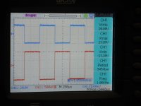
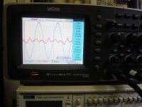
OK. Measured again the Sine and Square Wave of 1khz, still 20.8Volts output before the sine wave would really clip.
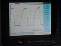
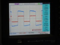
Switching the Frequency to 100KHz, again WOW, Clear as the 1KHZ Wave.
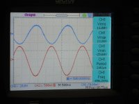
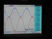
Turned Frequency up to 530KHZ till the output would drop down to 16Volts RMS. But no Clipping.
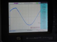
Slowly turned the function Gen backwards, and finally @300K there distortion was gone, and the full 20.0 Volts same as 1Khz where a there.
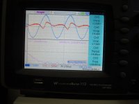
Now, it was still unbelievable. So I took a 1Kohm resistor and soldered this from Collector to GND.
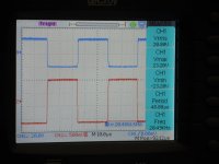
Now some changes happened. But still 20Volts RMS output at the collector of the Second Drive Transistor. So, lowered that 1K to 600 Ohms and I still got 17Volts output.
So I was very pleased and measured Noise, and Hum and DCV out and all was better that I thought it would be.
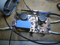
So, I decided to stop working on it, as it was already late night, and today I went back and checked everything because I thought I would connect the Power Transistors and the screwing the board on to the Heat sink. While getting the Drive Transistor in position to screw them onto the HEAT SINK, I saw something strange. The first Drive transistor had no number printed on front of it, or better say LABEL. I use BD139-10. this one are all PLASTIC.
So I took a multiplying lens and checked for the LABEL. and because of these two Transistors, are just besides each other I noticed that the thickness of the left one didn't match the right one, and then I looked at the backside of the left transistor, and there was the label. But hey, the amp was just running fine.
Connected the Amp again and tested again. same as last night exactly. just beautiful. Removed the Wires, dis-soldered that Transistor and used my TR TESTER to check HFE Gain, and it was I noted it down the other day when I made Selection of the Transistors. And one more thing was curious. Usually I need to get some small Capacitors soldered on BC to reduce parasitic noise, just a few Picofarad usually not larger than 33PF. but on this Board, I did not need any.
Of course, last night I took Pictures of the Scope and the measurements.
Then I saw in the pictures that the Transistor was running out of Phase by 180 Degrees, and this on all Frequencies.
So today, I soldered it back into the PCB, but this time the right way.
Set up my Instruments and tuned to 1KHZ sine Wave 50% output. first thing I saw, was lots of Parasitic Noise, two small Capacitors together 33 and 22 Pico and the wave was just as beautiful as last night.
I do always search for the max, so Pictures are taken @20.8 volt, where the Wave starts to clip. Sine 500K is 16Volts RMS, still within 2db without clip.
But the follow up was not that nice anymore. 1Khz to 50KHz 20Volts RMS before Clipping, with shunt resistor of 1KOhm to GND.
Above that just Catastrophic. 100KHZ -1db 120 - 2db no way to get higher than 150K would output only 16Volts RMS. Still good but not to compare with last night.
The BD139-10 pin layout is 1= Emitter 2= Collector 3= Base if seen from front where the label is printed. I soldered it with the label to the back, this would mean that E & B were reversed. So how the AMP POSSIBLE COULD work and WORK BETTER THAN when connected the RIGHT WAY.
Has anyone see something similar to this,??
Of course I have pics and I also will place the Circuit. But what you would say just out of the blue has happen. I tried to simulate that today on my computer, yea I could simulate it but with lost of distortion measured in the simulator software, but in real-time there wasn't any distortion.
Does anyone has an Idea,? Shall i put the Transistor the wrong way in to get better number? And after all the world would laugh at me, what a fool..
Thanks for any Input
Regards
Chris Hess
Look at the pics from Last night first. these from today
I will place later..
Everybody, I'm working on a Input and also Driver stage on a new Design for a Class A Amplifier.
The Point is this input is already build and it is running almost perfect.
Now nothing seems to be perfect,sometimes. as you will see..
I'm trying to increase the upper Frequency range of that Stage. This consists of 3 Transistors. It can be two as well, but if I use only two then I lose gain.
If I use three then Bandwidth will not Exceed 100Khz much. And output of Square Wave and also Sine wave will be Distorted, up to 1% comparing to 1Khz. The Circuit I have uploaded before already but I will upload it again, when I have Commented what has happen last night, in the circuit.
Now, this amplifier again with Output connected is build and it runs, but for my understanding there could be more. and has been tested already, and it sounds great, but I'm not finished with it yet.
Last night while testing and preparing the PCB, By accident, I reversed somehow the BASE and EMITTER Pins, of the first Drive Transistor. Put on my desk, plugged in my Test Equipment and tested just the output of the second Drive Transistor. This I tested OPEN LOOP, so none Negative Feedback as well Output Transistors weren't connected yet, and applied Power.
At that Time, this was last night, I didn't knew that I Reversed that Transistor, and started with 1KHz Sine Wave, and pulled up the Gain control on the Function Generator and measured Output on the Collector of the Second Drive Transistor with 25.6 Volt RMS! See Pic 10..
WOW!!! Why, what happen.??? I was stunned about that, so I viewed and controlled the RAIL VOLTAGES and there I thought I saw why, 48Volts, + and 48Volts -.
Oh, yes, of course, output Transistor hadn't been connected yet, OK clear.
So I connected a Load which would Simulate the Output Transistor to 70% and checked the Voltage again. DC V+- read both 43Volts sometimes only 42.9 but equal.
OK. Measured again the Sine and Square Wave of 1khz, still 20.8Volts output before the sine wave would really clip.
Switching the Frequency to 100KHz, again WOW, Clear as the 1KHZ Wave.
Turned Frequency up to 530KHZ till the output would drop down to 16Volts RMS. But no Clipping.
Slowly turned the function Gen backwards, and finally @300K there distortion was gone, and the full 20.0 Volts same as 1Khz where a there.
Now, it was still unbelievable. So I took a 1Kohm resistor and soldered this from Collector to GND.
Now some changes happened. But still 20Volts RMS output at the collector of the Second Drive Transistor. So, lowered that 1K to 600 Ohms and I still got 17Volts output.
So I was very pleased and measured Noise, and Hum and DCV out and all was better that I thought it would be.
So, I decided to stop working on it, as it was already late night, and today I went back and checked everything because I thought I would connect the Power Transistors and the screwing the board on to the Heat sink. While getting the Drive Transistor in position to screw them onto the HEAT SINK, I saw something strange. The first Drive transistor had no number printed on front of it, or better say LABEL. I use BD139-10. this one are all PLASTIC.
So I took a multiplying lens and checked for the LABEL. and because of these two Transistors, are just besides each other I noticed that the thickness of the left one didn't match the right one, and then I looked at the backside of the left transistor, and there was the label. But hey, the amp was just running fine.
Connected the Amp again and tested again. same as last night exactly. just beautiful. Removed the Wires, dis-soldered that Transistor and used my TR TESTER to check HFE Gain, and it was I noted it down the other day when I made Selection of the Transistors. And one more thing was curious. Usually I need to get some small Capacitors soldered on BC to reduce parasitic noise, just a few Picofarad usually not larger than 33PF. but on this Board, I did not need any.
Of course, last night I took Pictures of the Scope and the measurements.
Then I saw in the pictures that the Transistor was running out of Phase by 180 Degrees, and this on all Frequencies.
So today, I soldered it back into the PCB, but this time the right way.
Set up my Instruments and tuned to 1KHZ sine Wave 50% output. first thing I saw, was lots of Parasitic Noise, two small Capacitors together 33 and 22 Pico and the wave was just as beautiful as last night.
I do always search for the max, so Pictures are taken @20.8 volt, where the Wave starts to clip. Sine 500K is 16Volts RMS, still within 2db without clip.
But the follow up was not that nice anymore. 1Khz to 50KHz 20Volts RMS before Clipping, with shunt resistor of 1KOhm to GND.
Above that just Catastrophic. 100KHZ -1db 120 - 2db no way to get higher than 150K would output only 16Volts RMS. Still good but not to compare with last night.
The BD139-10 pin layout is 1= Emitter 2= Collector 3= Base if seen from front where the label is printed. I soldered it with the label to the back, this would mean that E & B were reversed. So how the AMP POSSIBLE COULD work and WORK BETTER THAN when connected the RIGHT WAY.
Has anyone see something similar to this,??
Of course I have pics and I also will place the Circuit. But what you would say just out of the blue has happen. I tried to simulate that today on my computer, yea I could simulate it but with lost of distortion measured in the simulator software, but in real-time there wasn't any distortion.
Does anyone has an Idea,? Shall i put the Transistor the wrong way in to get better number? And after all the world would laugh at me, what a fool..
Thanks for any Input
Regards
Chris Hess
Look at the pics from Last night first. these from today
I will place later..
Attachments
-
 1.Sine 1Khz 20.8 Volts RMS-s.jpg181.8 KB · Views: 178
 -
 PCB Measruring -s.jpg252.7 KB · Views: 75
 -
 8.Sine 500Khz 16VRMS-s.jpg181.3 KB · Views: 63
 -
 8. Sine 300Khz 20Vrms-s.jpg177.4 KB · Views: 62
 -
 6.. Square 100Khz 20.8 Votls RMS-s.jpg180.6 KB · Views: 60
 -
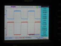 5. Square 50Khz 20.8 Volts RMS-s.jpg178.9 KB · Views: 56
 -
 5. Sine 50Khz 20Votls RMS-s.jpg184.3 KB · Views: 161
 -
 4. Square 20Khz 20Volts RMS-s.jpg179.8 KB · Views: 155
 -
 4. Sine 20Khz 20Volts RMS-s.jpg179.5 KB · Views: 156
 -
 1.Square 1Khz 20 Volts RMS-s.jpg180.1 KB · Views: 170
Supsicious.
First Thank you for responding,.
What you see now is completely not understandable.
The following pictures are taken 3 hours ago.. THESE ARE TAKEN FROM THE CORRECT INSTALLED TRANSISTOR.
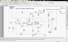
One Circuit I made as PDF this is the ORIGINAL ONE with everything correct and also Working with the Output connected. the second one is also working haven't tried what happen when the Output Transistors are connected, but I doubt that it don't work.
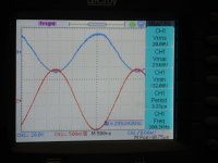
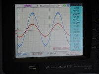
In the picture here you will see that both input and output are IN PHASE TO EACH OTHER, and I think this is WRONG because the first Transitor changes the Phase,.
Can not place all pictures.. Sorry need a next Reply for this.
In the circuit the Transistor Q21 is the correct way, and Q2 is the way the Spec is much better than the RIGHT and CORRECT way.. Everthing else is exactly the same. the components on the right side aren't connected in both cases.
Voltages are the same.
Any one is welcome to comment, I'm open to any comment. Thanks.
There is also a pic with the overall noise @ 86Volts Rail voltage.. 2x43
Thanks for reading.
Regards & Thank you for any comment.!
Chris
First Thank you for responding,.
What you see now is completely not understandable.
The following pictures are taken 3 hours ago.. THESE ARE TAKEN FROM THE CORRECT INSTALLED TRANSISTOR.
One Circuit I made as PDF this is the ORIGINAL ONE with everything correct and also Working with the Output connected. the second one is also working haven't tried what happen when the Output Transistors are connected, but I doubt that it don't work.
In the picture here you will see that both input and output are IN PHASE TO EACH OTHER, and I think this is WRONG because the first Transitor changes the Phase,.
Can not place all pictures.. Sorry need a next Reply for this.
In the circuit the Transistor Q21 is the correct way, and Q2 is the way the Spec is much better than the RIGHT and CORRECT way.. Everthing else is exactly the same. the components on the right side aren't connected in both cases.
Voltages are the same.
Any one is welcome to comment, I'm open to any comment. Thanks.
There is also a pic with the overall noise @ 86Volts Rail voltage.. 2x43
Thanks for reading.
Regards & Thank you for any comment.!
Chris
Attachments
-
 5. Distortion Parasitic noise wirhout Cap 50PF.jpg168.4 KB · Views: 67
 -
 8. Square Wave 100Khz 20Vrms.jpg166.1 KB · Views: 55
 -
 8. Sine Wave 100KHz 20Vrms.jpg162.9 KB · Views: 61
 -
 6. Sqaure 20Khz 20Vrms.jpg164.2 KB · Views: 61
 -
 6. Sine Wave 20Khz 20Vrms.jpg168.5 KB · Views: 53
 -
 2. Square 10Hz 20Vrms.jpg164.9 KB · Views: 63
 -
 2. Sine 10Hz 20Vrms.jpg166.1 KB · Views: 62
 -
 1. Square Wave 1KHz 20Vrms In Phase.jpg161.1 KB · Views: 77
 -
 1. Sine wave 1Khz 19.60 Vrms in phase.jpg163.4 KB · Views: 119
 -
 ScreenShot195.jpg397.6 KB · Views: 103
Last edited:
Nothing the amp just runs fine..
I actually placed Q2 for or to impedance changer that Q3 don't load Q1 too much,
Load of Q1 is about 300 Ohms and it heat it up, with Q2 in place I get 750 and more stable..
If Q2 is removed then I lose about 2 volts output and for an CLASS A Single end this is a lot.
Also the Resistor Cross on Collector of Q2 is reducing HUM and NOISE of overall performance by 20DB.. No joke. I can just lift collector of Q2 and the AMP still runs, but hum will increase quite much.
Now we have late night here in swiss, tomorrow morning I will place the outputs only 2 and then set Q2 the wrong way and measure and listen to it,, if it sounds better then I WILL KEEP THIS>
LOL
No, Just Joking I want to know why.
I can assure you, this one really brings it.. it has all what someone expect from a good amp..
On monday I get an REAL DISTORTION METER HP, and then we see what can be done to get hum, and noise,which still can be measured but not be heard, to even less than it is now.
Thanks.. It's appreciated..
Chris
Last edited:
If you remove Q2 and short the BE circuit connections (Q1 collector to Q3 base),
you get the same circuit behavior as with reversed BE for Q2, right?
you get the same circuit behavior as with reversed BE for Q2, right?
Last edited:
Removal of Q2 not an otpion right now.
You are right, and I have talked about that a few days back with somebody, then I have tested that and it turned out that it did't work. But this wasn't for that Reason, the reason for it was to use as little components as possible and still get good sound and good numbers.
Sorry, Remove Q2 is not an option at present time.. But I will give it a try in the morning.. let see what comes up. But you have seen when removing Q2 then it is very possible that Input and Output are out of Phase and this is not welcomed. But I give it try.. The layout of the board is made that many think can be changed without to have to destroy the board or to have to cut tracks.
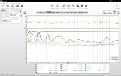
But I remember removing Q2 and everything degrades, see the REW PRINT SCREEN, directly coupled to the Amp output @8ohm.
First is without Q2, second one is with Q2. Check Noise Level on both.,.
Difference is 11% Noise and hum from the first to the second..
I'm appriciate your help very much. Tomorrow I post more Pics when Output Transistors have been added. and with the real Load, then you can see that this isn't that easy.
Have you heard of ZEN., one of the real good Amps of Nelson Pass
Have you heard of DoZ or DEATH of ZEN of Rod Elliot?
This amp here is something taken further than these two amps, further in the way using dual rail, using OCL, using higher Voltage, and using as litte as possible Capacitors in the sound PATH. Both of these amps are master pieces, and this Amp can't reach the quality of theses both, but it is single ended CLASS A and this already beats a lot of other amps.
this what has happen with that wrong inserted Transistor, wasn't expected that way and I have learned a lesson, and want to know why, that's all about.
and with the help of you guys here we will find the reason. one way or another..
With Q2 installed correctly or not doesn't matter, output noise with no signal input at present time is 0.2 to 1 millivolt. Removing Q2 it goes just up to 10 and more millivolts..
You are right, and I have talked about that a few days back with somebody, then I have tested that and it turned out that it did't work. But this wasn't for that Reason, the reason for it was to use as little components as possible and still get good sound and good numbers.
Sorry, Remove Q2 is not an option at present time.. But I will give it a try in the morning.. let see what comes up. But you have seen when removing Q2 then it is very possible that Input and Output are out of Phase and this is not welcomed. But I give it try.. The layout of the board is made that many think can be changed without to have to destroy the board or to have to cut tracks.
But I remember removing Q2 and everything degrades, see the REW PRINT SCREEN, directly coupled to the Amp output @8ohm.
First is without Q2, second one is with Q2. Check Noise Level on both.,.
Difference is 11% Noise and hum from the first to the second..
I'm appriciate your help very much. Tomorrow I post more Pics when Output Transistors have been added. and with the real Load, then you can see that this isn't that easy.
Have you heard of ZEN., one of the real good Amps of Nelson Pass
Have you heard of DoZ or DEATH of ZEN of Rod Elliot?
This amp here is something taken further than these two amps, further in the way using dual rail, using OCL, using higher Voltage, and using as litte as possible Capacitors in the sound PATH. Both of these amps are master pieces, and this Amp can't reach the quality of theses both, but it is single ended CLASS A and this already beats a lot of other amps.
this what has happen with that wrong inserted Transistor, wasn't expected that way and I have learned a lesson, and want to know why, that's all about.
and with the help of you guys here we will find the reason. one way or another..
With Q2 installed correctly or not doesn't matter, output noise with no signal input at present time is 0.2 to 1 millivolt. Removing Q2 it goes just up to 10 and more millivolts..
Attachments
Last edited:
Q2 is acting like a zener 6 -7 v reverse accross the B-E junction making it a *wierd* two stage design as the collector connection may have an effect.
measure the DC voltage accross R24 when the transistor is in wrong
R24 should see 1.4 - 1.6v when Q2 is correctly installed
measure the DC voltage accross R24 when the transistor is in wrong
R24 should see 1.4 - 1.6v when Q2 is correctly installed
Last edited:
Thanks for your answer
I have tought of something like that before . I'm running a version without Collector Pin connected to RAIL, it has a fantastic sound, but it created hum.. Installing RC 100 Ohm it revomes any noise and hum the amp has, but it also crops the Sine wave above 50khz and really badly..
Installing a Resistor 500Ohm together with a resistor from Collector to GND, i,e 250 Ohm, if the amp Clips then transistor burns, the COllector Resistor to Rail burns instantly, even a 3 WATT...
Installing a Resistor 1k so as seen in circuit and another to GND with 250 Ohm and everything is fine, no crop of high Frequencies, no melt down no transistor short out even driven into CLIP by double voltage at the output which the amp is able to deliver. I use for each channel 25AMP Transformers. and Idle is somewhere at 5+ amp
Regards
chris
OK Guys
I just come out of my Working room. BTW it's 2:33 Am
Following I did
Removed Q2
Made a direct connection from Q1 C to Q3 Base
Added 47uf 50 Volts to Outleg of Resistor RV100K which connects to Trimpod 1st pin, to filter Ripple which could eventually come from PSU.
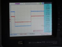
Started the AMP and the first task was shorted the input to GND and Measured Collector of Q3 found to have 16mv @ 106Hz Ripple. for me too much as with Q2 installed it's only 0.2 - 1.0 mv maximum.
Checked frequency same as you have seen in the pics.
Have to say, its non inverting, meaning in Phase. 20Volts RMS for all up to 120 KHz. then it sligthly drops down to -1dB for 200Khz
This way I could accept to operate that amp if It doesn't hum and does not imply noise, which we will know in the morning.
But these 16 millivolts must go down.. have to find a way to get rid of this...
But all in all it may work out.. and this is your HELP Guys
For now Thank you..
See you tomorrow, for me in the morning,..
Regards from capital City of Switzerland
Chris Hess
I just come out of my Working room. BTW it's 2:33 Am
Following I did
Removed Q2
Made a direct connection from Q1 C to Q3 Base
Added 47uf 50 Volts to Outleg of Resistor RV100K which connects to Trimpod 1st pin, to filter Ripple which could eventually come from PSU.
Started the AMP and the first task was shorted the input to GND and Measured Collector of Q3 found to have 16mv @ 106Hz Ripple. for me too much as with Q2 installed it's only 0.2 - 1.0 mv maximum.
Checked frequency same as you have seen in the pics.
Have to say, its non inverting, meaning in Phase. 20Volts RMS for all up to 120 KHz. then it sligthly drops down to -1dB for 200Khz
This way I could accept to operate that amp if It doesn't hum and does not imply noise, which we will know in the morning.
But these 16 millivolts must go down.. have to find a way to get rid of this...
But all in all it may work out.. and this is your HELP Guys
For now Thank you..
See you tomorrow, for me in the morning,..
Regards from capital City of Switzerland
Chris Hess
The Understanding and correction of that Error
Guys,
Just to keep my promise, I'm back right here,.,
New is that I changed, or say better reversed that Second Drive Transistor to be correct. the I removed that 1K Collector Resistor, and let the 250Collector Resistor connected to GND.
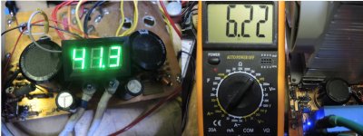
and now all is working as expected, HUM and Noise is no more a Question, MAX VDC Output at full Load 8 Ohms, 4 Ohms or even 2 Ohms, is down to max 12mv.. usually it's 0.000
I have to split the Pictures for this one, because Part of is actually for my other Thread,, Building a Class Amplifier from Scratch.. So I just place the Read out of that Amp today, and the rest in my other Thread.. You can find here:
Building a Class Amplifier from Scratch
So that's about it..
The read out I made Today and Results of Read out is according as you can See in the Pictures From Today,
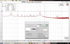
Any input is welcome.. Output Power would be more, than you can see, if I would drive that Amp in 1% distortion, which actually no one hears, but I do not like that too much and so it's 20Watt @ Distortion of 0.245% for 1LKhz and 0.86% @ 100KHz. all in the range of .5DB
Any Question Just ask.
Transistor in the circuit Q2 is a must for Stability and Less Noise.! Even Circuit looks Odd and weird, without that amp is not HQS = High Quality Sound or High End..
Thanks.
Chris Hess
Guys,
Just to keep my promise, I'm back right here,.,
New is that I changed, or say better reversed that Second Drive Transistor to be correct. the I removed that 1K Collector Resistor, and let the 250Collector Resistor connected to GND.
and now all is working as expected, HUM and Noise is no more a Question, MAX VDC Output at full Load 8 Ohms, 4 Ohms or even 2 Ohms, is down to max 12mv.. usually it's 0.000
I have to split the Pictures for this one, because Part of is actually for my other Thread,, Building a Class Amplifier from Scratch.. So I just place the Read out of that Amp today, and the rest in my other Thread.. You can find here:
Building a Class Amplifier from Scratch
So that's about it..
The read out I made Today and Results of Read out is according as you can See in the Pictures From Today,
Any input is welcome.. Output Power would be more, than you can see, if I would drive that Amp in 1% distortion, which actually no one hears, but I do not like that too much and so it's 20Watt @ Distortion of 0.245% for 1LKhz and 0.86% @ 100KHz. all in the range of .5DB
Any Question Just ask.
Transistor in the circuit Q2 is a must for Stability and Less Noise.! Even Circuit looks Odd and weird, without that amp is not HQS = High Quality Sound or High End..
Thanks.
Chris Hess
Attachments
-
 9. Raila & Current.jpg330.5 KB · Views: 59
 -
 8. 100Khz - 8Ohm Full Load & distortion.jpg317.3 KB · Views: 59
 -
 7. 20Khz - 8Ohm @Full Power 0.34% Distortion.jpg151.8 KB · Views: 63
 -
 6. 20Khz - 8Ohm @Full Power.jpg142.9 KB · Views: 60
 -
 5. 10Khz - 8Ohm @full Power 0.375%.jpg155.4 KB · Views: 85
 -
 4. Distortion 10Khz 8Ohm @Full Power.jpg136.9 KB · Views: 76
 -
 3. DCV out at Speaker Terminal @Full Load 1Khz 8Ohm.jpg146.3 KB · Views: 86
 -
 2. THD Measured @full Power HP331A !Khz 8Ohm less than 0.245%.jpg165.2 KB · Views: 111
 -
 1. THD Class A Single End @full Power 8Ohm 1Khz.jpg154.3 KB · Views: 103
 -
 10. 100Khz - 8 Ohm FFT Test, with Distortion @ full Load less than 1%.jpg150.3 KB · Views: 83
The Final Circuit - Class A
So guys, I have finally solved the the problem with Transistor 2. And all the bad "things, decrease from high frequencies - above 50khz."
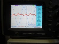
Not only this, also the transistor is still in the circuit, and this time there is no PHASE SHIFT, it just goes up to 150Khz within .1db seeing it relevant to 1Khz.
Distortion is measured all over the frequency Band with .1 it stays like that for terms of 1WATT as also in terms for full load at about 20 watts "it's 23Watts @8 Ohm"
But the major part of what I got is, no more HUM on the circuit.
Noise is down with open or closed input to 0.1 - 0.3 Milli-volt RMS.
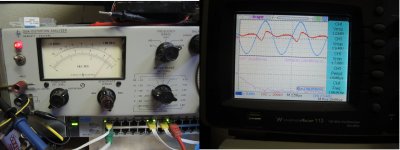
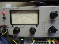
Circuit runs with RAIL VOLTAGE from +- 32 Volts to +- 42 Volts with 7.5 Emitter Resistor. Distortion is measured with HP331A Distortion Analyzer.
Load was DUMMY LOAD as well as REAL 8Ohm. and 4 Ohm Speakers for all measurements.
Current Draw is about 5.5 Ampere / Channel @+-42Volts Rail and 4.2Ampere /Channel @+-32 Volts Rail.
Heat is 50 Degrees C for the 32V version and 80degrees C for the 42Volt Version. Fan is a must on these Active Heat-sinks. Low turning noise of Fan increases over all noise by 8db.
Will place some soundcheck and also pictures for that LAST Prototype of this Amp later tonight.. now we have 8:33 here in Swiss..
Enjoy and have a nice Day.
Regards Chris Hess
So guys, I have finally solved the the problem with Transistor 2. And all the bad "things, decrease from high frequencies - above 50khz."
Not only this, also the transistor is still in the circuit, and this time there is no PHASE SHIFT, it just goes up to 150Khz within .1db seeing it relevant to 1Khz.
Distortion is measured all over the frequency Band with .1 it stays like that for terms of 1WATT as also in terms for full load at about 20 watts "it's 23Watts @8 Ohm"
But the major part of what I got is, no more HUM on the circuit.
Noise is down with open or closed input to 0.1 - 0.3 Milli-volt RMS.
Circuit runs with RAIL VOLTAGE from +- 32 Volts to +- 42 Volts with 7.5 Emitter Resistor. Distortion is measured with HP331A Distortion Analyzer.
Load was DUMMY LOAD as well as REAL 8Ohm. and 4 Ohm Speakers for all measurements.
Current Draw is about 5.5 Ampere / Channel @+-42Volts Rail and 4.2Ampere /Channel @+-32 Volts Rail.
Heat is 50 Degrees C for the 32V version and 80degrees C for the 42Volt Version. Fan is a must on these Active Heat-sinks. Low turning noise of Fan increases over all noise by 8db.
Will place some soundcheck and also pictures for that LAST Prototype of this Amp later tonight.. now we have 8:33 here in Swiss..
Enjoy and have a nice Day.
Regards Chris Hess
Running a transistor with base-emitter junction reverse-biased into zener breakdown will at best make it noisier that it was before, and often destroys the device. Best to replace the device as its performance and reliability may be compromized.
Since the component in question was an emitter-follower to boost the current handling its not surprizing that you could get some sort of functionality mis-wired as their only needed to be some sort of conduction across it to complete the feedback loop. Until the output is heavily loaded the current gain of that stage might not be needed...
Since the component in question was an emitter-follower to boost the current handling its not surprizing that you could get some sort of functionality mis-wired as their only needed to be some sort of conduction across it to complete the feedback loop. Until the output is heavily loaded the current gain of that stage might not be needed...
Project has been finished quiet good. Thank you all
Hi Mark
You are completely right. In every aspect.
And do not misunderstand me, we are talking here from a PURE CLASS A in every aspect. Without CURRENT SOURCE Transistors. If you looked at the Circuit then you will notice that all is straight forward.. The only "NEGATIVE FEEDBACK" is the Gain Control R7 & R8. this is set to 510Ohms and 41Ohms. Gain is about 13, it's possible to lower this. But not below 10, then we will loose high frequencies.
As I stated earlier and in the first post of this thread here, this was an ACCIDENT that the Transistor got reversed. Earlier Days I used BD139 with the metal Back where you would need some MICA between the transistor and the heat sink. These transistors which I got this time are all PLASTIC, no need for MICA. and there is the source of the Error. As the prints are very thin and almost invisible, on the front side of the transistor.
In fact Q2 is just a impedance Changer between Q1 and Q3 and without any GAIN. at least in this configuration. That's one part of the work this Transistor needs to do.
The second part this Transistor does is much more Important as I found out and that's why the Transistor stays in that Circuit. It does something, CR Filters nor LC or CLR filters can provide better than this only one Transistor.
To run this AMP without HUM it takes a power-supply with 100MILLIFARAD = 0.1FARAD Capacitors, each of this cost 60USD and I would need 4 of them.
Then I need 4 Chokes Donuts (I got them here at Home) with just 100Micro Henry 10Ampere /Piece and a few Resistors. but these Chokes are also 20USD one piece. That is very costly, even usually if there is no other way, then I am willing to pay the prices..
But this only one BD139 cost me 80 Cents, only and he reduces HUM BY 50DB.!
If I build a PSU with the components above I will get 67millivolts Hum @50 hertz and less than 5 Millivolts at 100Hz. But is cost almost 500US$!!
Now this blows right into the Collector Pin of Q1 and into Collector Pin of Q3, with 67Millivolts then when there is open Input or closed input, and it doesn't matter the AMP will show HUM. Even it's almost impossible to hear, but taking a fast Low frequency driver and we can hear that hum, and of course as you can see of the REW Printout the computer can also see it.. and hear it..
Placing that BD139 in between Q1 and Q3 reduces all these problems. the PSU can have 800Millivolts RIPPLE and never mind how fast that Low Frequency Speaker Driver is, it does not HUM any more.
And REW will measure 50db less. but look a the configuration of that Transistor as it only works that way, meaning connecting that collector with 250Ohms to GND, getting 1K to Rail+ and get between 1.1K and 3k to Emitter Pin of this Transistor. The Emitter Resistor also has influence on high Frequencies above 50KHZ, the larger it goes up the better is the response. and the clearer is the sound. But it maxes out depending on HFE @3kohm
The 6 Parallel OUTPUT transistor VERSION of this Amp I placed in the box last night after testing it for 30 Days outside the BOX, and again it's a step into the right direction to come as close as possible to the REAL SOUND. With this I mean Natural sound, sound reproduction of the fine ART. This is my goal.
I drew a new Circuit basing on this one here improving Output Performance by about 3Volts in GAIN INCREASE by increasing Vrail + - to 60 volts for the FRONT STAGE.
But keeping the Driver and output stage at Vrail +-42Volts
This will force me to have the TOROIDS made especially for me as there are two more Winding needed.
But for the Time being, for me the best Sound of an Amplifier I ever made.
I have to say Thanks to NELSON PASS for his indirect HELP he provided to me, since I started with this AMP.
Now that Amp is finished, the project of that Class A has been achieved more than I thought I could. And believe me it sounds good. Natural.
I have a new one in the pipeline... and working on it. But the next one will be with PASSIVE HEAT SINKS.. I know it will cost a fortune..
Circuit of this one here including LAYOUT FILES which I will place in a FINAL POST coming soon. I'm working on it. But honestly I'm quite tired at present time, not of Electronics, but on the circumstances world is in right now.
But building this Amp is not inexpensive, even the 2 Transistor version will be around 500US$ per channel if anyone is buying good Parts, or may the prices are only high in Swiss..
Transformers under 750VA will not work proper for that AMP. and I'm talking about per Channel.
The nice thing on that AMP is the builder can use any VOLTAGE from +-30Volts 10AMPS up to +- 42Volts 10Amps/Side without to have to adjust anything..
Have to explain that Indirect Help of NELSON PASS.. He never said, do this do that, or use this or use that Except one time when it concerned the Second Harmonic Distortion Wave Form.. He wrote, you need to check 2nd Harmonic, many people they do not check the 2nd, I do...
For everything else he just wrote, something like that: Go for it it's all fun. Do it, and gave some samples about what he had done in earlier days, so this is called inspiration. and therefor I like to express my thanks again to the only one Master of Amps NELSON PASS. Things like that would never happen in Europe, and especially not in Swiss. I'm still overwhelmed about that friendliness of him
Mark and everybody else, Thanks for your Input..
Without your guys I would never finish this
Regards and Respect to all of you..
Chris Hess
Last edited:
Project has been finished quiet good. Thank you all
Hi Mark
You are completely right. In every aspect.
And do not misunderstand me, we are talking here from a PURE CLASS A in every aspect. Without CURRENT SOURCE Transistors. If you looked at the Circuit then you will notice that all is straight forward.. The only "NEGATIVE FEEDBACK" is the Gain Control R7 & R8. this is set to 510Ohms and 41Ohms. Gain is about 13, it's possible to lower this. But not below 10, then we will loose high frequencies.
As I stated earlier and in the first post of this thread here, this was an ACCIDENT that the Transistor got reversed. Earlier Days I used BD139 with the metal Back where you would need some MICA between the transistor and the heat sink. These transistors which I got this time are all PLASTIC, no need for MICA. and there is the source of the Error. As the prints are very thin and almost invisible, on the front side of the transistor.
In fact Q2 is just a impedance Changer between Q1 and Q3 and without any GAIN. at least in this configuration. That's one part of the work this Transistor needs to do.
The second part this Transistor does is much more Important as I found out and that's why the Transistor stays in that Circuit. It does something, CR Filters nor LC or CLR filters can provide better than this only one Transistor.
To run this AMP without HUM it takes a power-supply with 100MILLIFARAD = 0.1FARAD Capacitors, each of this cost 60USD and I would need 4 of them.
Then I need 4 Chokes Donuts (I got them here at Home) with just 100Micro Henry 10Ampere /Piece and a few Resistors. but these Chokes are also 20USD one piece. That is very costly, even usually if there is no other way, then I am willing to pay the prices..
But this only one BD139 cost me 80 Cents, only and he reduces HUM BY 50DB.!
If I build a PSU with the components above I will get 67millivolts Hum @50 hertz and less than 5 Millivolts at 100Hz. But is cost almost 500US$!!
Now this blows right into the Collector Pin of Q1 and into Collector Pin of Q3, with 67Millivolts then when there is open Input or closed input, and it doesn't matter the AMP will show HUM. Even it's almost impossible to hear, but taking a fast Low frequency driver and we can hear that hum, and of course as you can see of the REW Printout the computer can also see it.. and hear it..
Placing that BD139 in between Q1 and Q3 reduces all these problems. the PSU can have 800Millivolts RIPPLE and never mind how fast that Low Frequency Speaker Driver is, it does not HUM any more.
And REW will measure 50db less. but look a the configuration of that Transistor as it only works that way, meaning connecting that collector with 250Ohms to GND, getting 1K to Rail+ and get between 1.1K and 3k to Emitter Pin of this Transistor. The Emitter Resistor also has influence on high Frequencies above 50KHZ, the larger it goes up the better is the response. and the clearer is the sound. But it maxes out depending on HFE @3kohm
The 6 Parallel OUTPUT transistor VERSION of this Amp I placed in the box last night after testing it for 30 Days outside the BOX, and again it's a step into the right direction to come as close as possible to the REAL SOUND. With this I mean Natural sound, sound reproduction of the fine ART. This is my goal.
I drew a new Circuit basing on this one here improving Output Performance by about 3Volts in GAIN INCREASE by increasing Vrail + - to 60 volts for the FRONT STAGE.
But keeping the Driver and output stage at Vrail +-42Volts
This will force me to have the TOROIDS made especially for me as there are two more Winding needed.
But for the Time being, for me the best Sound of an Amplifier I ever made.
I have to say Thanks to NELSON PASS for his indirect HELP he provided to me, since I started with this AMP.
Now that Amp is finished, the project of that Class A has been achieved more than I thought I could. And believe me it sounds good. Natural.
I have a new one in the pipeline... and working on it. But the next one will be with PASSIVE HEAT SINKS.. I know it will cost a fortune..
Circuit of this one here including LAYOUT FILES which I will place in a FINAL POST coming soon. I'm working on it. But honestly I'm quite tired at present time, not of Electronics, but on the circumstances world is in right now.
But building this Amp is not inexpensive, even the 2 Transistor version will be around 500US$ per channel if anyone is buying good Parts, or may the prices are only high in Swiss..
Transformers under 750VA will not work proper for that AMP. and I'm talking about per Channel.
The nice thing on that AMP is the builder can use any VOLTAGE from +-30Volts 10AMPS up to +- 42Volts 10Amps/Side without to have to adjust anything..
Mark and everybody else, Thanks for your Input..
Without your guys I would never finish this
Regards and Respect to all of you..
Chris Hess
- Home
- Design & Build
- Construction Tips
- Strange Occurance in Input of Driver Stage Class A