Folks:
I’m no engineer and could use some help. I’m building a preamp and would like to have a simple power off indicator. The preamp will have a 5VDC supply that is on at all times and a separate 5VDC supply that is only on when the preamp is “on” (i.e., not in standby mode). I’d like to include a front panel mounted LED that is only on when the preamp is in standby mode. Can anyone suggest a circuit?
Many thanks!
Regards,
Scott
This should do it.
Any NPN Bipolar (BC109 etc) will work.
Power on in ON mode and no LED. Power on in Standby mode and lit LED.
Any NPN Bipolar (BC109 etc) will work.
Power on in ON mode and no LED. Power on in Standby mode and lit LED.
Attachments
Last edited:
This should do it.
Any N channel FET or indeed NPN Bipolar (BC109 etc) will work.
Power on in standby mode and no LED. Power on in working mode and lit LED.
Flip the LED around.

Definitely.
However there is possibly a simpler circuit with the LED and resistor between the two supplies - might work, but has a danger of pulling up the switchable supply when its supposed to be off, depending on what else loads it down.
However there is possibly a simpler circuit with the LED and resistor between the two supplies - might work, but has a danger of pulling up the switchable supply when its supposed to be off, depending on what else loads it down.
Half asleep as usual, forgot to add R5. R2 is required across the LED to ensure it is not glowing when off.
The placing of an LED between thhe two rails will not allow Standby to function properly as the current, 10mA ish, will always flow and keep the preamp running.
The placing of an LED between thhe two rails will not allow Standby to function properly as the current, 10mA ish, will always flow and keep the preamp running.
Attachments
I think the leakage current of Q2 will be in the nanoamp range unless it is very hot, not sure R2 is needed, and it can be much larger in value anyway.
Folks:
I've run into a bit of a snag: the attenuator system that I thought would provide 5 VDC only when it was "on" (i.e., not in standby mode) is actually providing about 2 VDC. The 2 VDC is insufficient to trigger the circuit JonSnell so kindly provided. I've contacted the attenuator systems' supplier (I'm building 2 preamps and am having the same issue with both) to determine if there's a way to increase the 2 VDC to 5 VDC. In the meantime (and especially if his answer is "no"), is there a simple fix?
Once again, many thanks!
Regards,
Scott
Attachments
Yes there is a simple fix. To avoid ambiguity and misunderstanding of "this newest revision of the design problem", please create a table with four rows similar to the following:
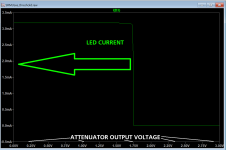
MODE V_Supply_1 V_Supply_2 LED_desire =========================================== A 11.3V 0.2V OFF B 11.3V 2.1V ON C 1.5V 0.2V OFF D 1.5V 2.1V ONMade a guess about what might be contained within the table of spec numbers and came up with this (simulated) result. Attenuator voltage is plotted on the X-axis, while LED current is on the Y-axis.
I used two junkbox BJTs (2N3904) for lots of DC gain and thus, reasonably steep transition region. 2*BJT + 1*LED + 5*resistor . When attenuator voltage is "low", LED is on. When attenuator voltage becomes "high", LED is off.
_
I used two junkbox BJTs (2N3904) for lots of DC gain and thus, reasonably steep transition region. 2*BJT + 1*LED + 5*resistor . When attenuator voltage is "low", LED is on. When attenuator voltage becomes "high", LED is off.
_
Attachments
Mark:
Okay, this should be informative! I've tested the B1 Rev 2 with the following results:
Is there another "Mode" test I should have performed as well?
Regards,
Scott
Okay, this should be informative! I've tested the B1 Rev 2 with the following results:
| Mode | Regulated Power Supply | Switched Source | LED Status |
| Standby | 5.01 VDC | 0 VDC | On |
| "On" | 5.01 VDC | 1.96 VDC | Off |
| [Attenuator bypassed, Reg PS connected to the "Switched Source"] | |||
| Bypassed | 5.01 VDC | 5.01 VDC | Off |
Is there another "Mode" test I should have performed as well?
Regards,
Scott
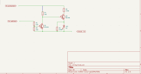
I think post #12 above, happens to implement your table EXACTLY. But you check it; you're the customer. I have assumed "Switch Source" and "Attenuator" are two names for the same thing.
Last edited:
Mark, et. al.:
I've been in contact with the diyAudio member who supplied me with the attenuator / input selection / display systems for the two B1 buffer projects I'm working on, and it seems I completely misunderstood how to use the 5 VDC "Switched Source" his system provides. He has advised me that the Switched Source cannot power the LED circuit above, but instead should be connected to the base of a transistor. I think I understand the concept -- the transistor base controls the connection between that transistor's collector and emitter, allowing 5 VDC supplied to the collector to pass through to the emitter and then on to the LED circuit. If my understanding is correct, what type of transistor should be used? I have a decent stock but don't know how to select amongst PNP vs. NPN and BJT vs. FET options.
Regards,
Scott
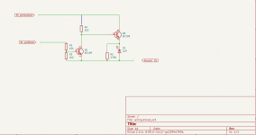
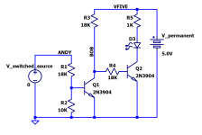
Here's the schematic which gives the simulation results in post #12. The Switched Source ("Attenuator") drives an the base of transistor Q1 through an 18 Kohm series resistor. I am confident the guy who supplied you with the attenuator system for B1 projects, will approve.
The resistor ratio (R1 / R2), along with the VBE of Q1 , sets the voltage at which the LED switches from off to on.
R3 and R4 prevent the circuit from drawing too much power from the 5 volt supply. Their values are noncritical, and it turns out everything works fine if you set them both to 18K , the same as R1. We in the business call this "BOM Line-Item Minimization"
R5, the forward voltage of LED D3, and the 5V power supply voltage, set the LED current and thus the LED brightness. To decrease brightness, increase R5. To increase brightness, decrease R5.
Q1 and Q2 are 2N3904 junkbox NPNs. If your junkbox happens to contain 2N2222A or BC547 or 2N4403 or BC337-40 etc, use those and it'll work. Just check and double check the pinouts, they are all different.
Attachments
Many meatballs?
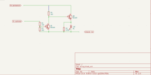
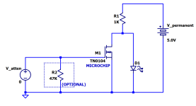
Minimalists may prefer a circuit having three components instead of eight. And here it is. However I doubt that your junkbox contains a logic-level-MOSFET in a TO92 package; so you may need to add this to your next Mouser or DigiKey order.
The circuit dissipates DC power at all times; current flowing through R1 is either (Vpermanant / R1) or else ((Vpermanent - Vfwd) / R1) but it's never zero. So to avoid the embarrassment of excess power consumption, the thing to do is maximize R1. That means choosing a high brightness LED which can be operated at very low current and still shine brightly. I recommend picking an LED whose datasheet spec for luminous intensity is greater than 10,000 millicandelas. For example, part number INL-3AG30 (link) is rated 18,000 millicandelas and costs USD 0.34 in quantity one. If you used this high brightness LED, it would allow you to set R1=6.2K and reduce power consumption.
The optional bleeder resistor R2 is unnecessary but possibly provides peace of mind. During initial debug and prototyping, if you're repeatedly connecting and disconnecting this LED status circuit to the attenuator system, and if you worry about ESD or other unhappy events, R2 keeps the MOSFET gate in its comfort zone: discharged to Vgs=0. Minimalism or safety, your choice.
_
Attachments
- Home
- Design & Build
- Electronic Design
- Standby Mode Indicator