Back again!
I need to drive a pair of (power!) P and N mosfet, source to ground, from LM319 comparator at + and - 10V. I already try 1.5K pull up resistor and a pair of PNP and NPN transistor as buffer, but near maximum duty cycle, this seem unsuficient...I try a TC4420 ( at 20V), this work very well, but its over the maximum rating of manufacturer....Anybody has already do some discret and SIMPLE driver that can provide + and minus 10 to 15V to drive mosfet?
Thanks
Fredos
Yeah it's for a class d amplifier!
Fredos,
Did you tried using IRFD9110/110 complementary mosfets in Common source configuration to drive the large power mosfets!!!
Amazed to see a guy capable of designing KW level PWM amps is searching here on this forum for drivers..........😉
Kanwar
Did you tried using IRFD9110/110 complementary mosfets in Common source configuration to drive the large power mosfets!!!
Amazed to see a guy capable of designing KW level PWM amps is searching here on this forum for drivers..........😉
Kanwar
Thanks for reply...
alfsch
That's exactly the way I have try, but at 250Khz with a LM319, at maximum duty cycle, I can't drive correctly mosfet...It work very well with a TC4420, but I'm over maximum rating of IC....
Workhorse
I have already try the source follower, but with voltage drop I can't bring power mosfet in full saturation...I have try common drain configuration with reverse input on my comparator, but introduce too much delay in rise and fall time....I'm looking to design a class d with less than 100ns response time...just the LM319 introduce nearly 40 ns, TC4420 35 ns, and mosfet itself nearly 40 ns....So with TC4420 solution, I'm out of my spec...With a pair of PNP and NPN driving transistor, I can reach my goal...But prob at maximum duty cycle....
At least, I will simply limit duty cycle and raise PSU voltage to keep same power....
Thanks
Fredos
Hi, Alfsch,
Interesting design 😀 ClassD version of Transnova. How to adjust the dead time in your design?
Interesting design 😀 ClassD version of Transnova. How to adjust the dead time in your design?
I don't understand how a direct coupled gate-drive circuit can exhibit duty-cycle-dependent performance.
fredos said:class d with less than 100ns response time...just the LM319 introduce nearly 40
Isn't LM319 a bit slow if you want less than 100ns total response time?
And please try to be more specific what is exactly your problem with high dyty cycles?
#lumanauw: depending on gate-drive /resistors you get a slew rate , about 0,5v/ns at the gates; from +4 to -4 v , one fet closing, other gets on, about 16ns "dead-time" ; using res+diode at gates you can adjust the dead-time even more;
and fets switch off faster , because negative driven
next is, because there is some stray ind. between the windings of the fets, the shoot, if any, is much smaller...
the problem is, you need n + p fets, so its only for small amps, lets say max. +/- 40v, with 100v fets like irf540/9540
and fets switch off faster , because negative driven
next is, because there is some stray ind. between the windings of the fets, the shoot, if any, is much smaller...
the problem is, you need n + p fets, so its only for small amps, lets say max. +/- 40v, with 100v fets like irf540/9540
Hi, Alfsch,
Nice 😀 Did you eventually built it? I noticed something. The feedback is taken after the LC filter. Is this UcD?
The parameter difference between Nch (IRF540) and Pch (IRF9640), will this be a problem in real cct?
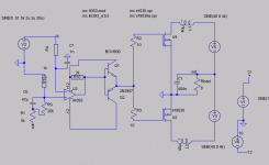
Hi, Fredos,
Q4-Q5=common collector bipolars, driving Q2-Q3=common source mosfets, and the drains are driving Q1 (the big mosfet)
Nice 😀 Did you eventually built it? I noticed something. The feedback is taken after the LC filter. Is this UcD?
The parameter difference between Nch (IRF540) and Pch (IRF9640), will this be a problem in real cct?
Hi, Fredos,
Q4-Q5=common collector bipolars, driving Q2-Q3=common source mosfets, and the drains are driving Q1 (the big mosfet)
Attachments
alfsch said:hi fredos,
a year ago i had this in mind: (pic)
you think about something like this?
for small mosfet, as trans i tried: bc516/17 , 1A darling
for bigger gates, komp.fet driver: irf7389 , 30v, 30a peak
monster , fast driver: tc4422
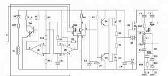
There is a problem with that in that there is nowhere for the inductors to reset when you turn the mosfets off.
Here you go....
Link
DNA
There is a problem with that in that there is nowhere for the inductors to reset when you turn the mosfets off.
coil "reset" < back-diodes
but for stray-ind. a extra snubber is needed, right, not in my pic...
is this, what you guessed?
btw, in the linked patent, i cannot see, why there should be "reduced ripple"...every d-amp has a coil between switching-stage and supply (and most times also a load), what is different here??
lumanauw said:Hi, Genomerics,
It's your patent? 😀
Guilty....
Hi Alfsch, erm... don't know. Don't tell me I might patent it. The reduced ripple current is demonstrated in the pictures.
Yo Fredos.... Attaching pictures doesn't usually work for me so I don't suppose this time will be any different.
You might try a HC, cmos, octal buffer. Use two gates as an input and parallel the other six to drive the emitters of a pair of grounded base NPN/PNP transistors. Collectors up/down to gates of a pair of PMOS/NMOS jobs and drains connected to get your final output.
If you use a tri-state device then you have a means of disabling the driver under fault conditions....
And..... you might be able to use the input gate threshold as your comparator.
DNA
The key for ripple current reduction and a completely different current consumption pattern from the power supplies (in comparison with the classic circuit) seems to be this capacitor across the drains of the MOSFETs. My guess is that it forms a LC filter together with the leakage (not coupled) inductance of the coil and prevents the current from shifting completely from one half of the coil to another after each switching event.
Funny approach. It may even be inmune to supply pumping. Can anybody confirm this?
Funny approach. It may even be inmune to supply pumping. Can anybody confirm this?
It started out as a 'what if' on the basis that in switch mode power supplies nodes in series with the inductor only see the ripple current.
The capacitor ended up in there as a path for inductor reset.....
Even though it might save the main resevoir caps from getting hammered that coupling capacitor gets it anyway.
After I'd done a bit of preliminary research to see if it was 'new' I went and filed the patent.
Afterwards I came across this
Link
So, as things turn out it is a Cuk derived topology. They still granted it even though I pointed out the similarity.
No..... it does not overcome power supply pumping.
DNA
Then again.... although it still suffers from power supply pumping you can use it to correct for the problem.
Since it causes the problem in the first place you can.....
Ground the sources through a small resistor and tie an average current mode control loop around things driven from something that senses the rail offset.
It is added complexity but the implementation might be simpler than other methods.
In the paper by Cuk he mentions a battery charger/discharger. Same thing here.
Have a look at figure 12)
If you rotate it 90 degrees and reconnect the load where we are used to putting it in a Class-D amplifier then you'll see......
DNA
Does this really pay back?
- Supply rail pumping would be similar as in a half bridge.
- Even if there is a reduced supply ripple (still do not see it....)... Even then a P-Chanel needs 3 times more silicone than N-Chanel.
-The reduced gate drive costs will be eaten up quite fast by the higher MosFet prices.
-You need two coupled inductors.
-Ripple current is not a big deal for low power designs.
Fredos, you must make your living from your designs.
Don't let me go dead as a dump head, -where is the economical clue?
I don't know about the economics.....
As you say the GB patent version I posted does not overcome supply rail pumping.
The reduction in supply ripple current does occur as suggested. In a normal half bridge the power supplies are subjected to a discontinuous, on off, current demand at the switching frequency as well as that due to the audio signal. In the modified version the current is continuous/triangular at the level of the inductor current.
You are, of course, right about the relative cost/performance of P-channel mosfets. The circuit could be implemented using a pair of N-channel devices but that would mean introducing level shifting and dead-time control. With a P-N pair level shifting is not required and dead-time is, more or less, eliminated. The possibility of cross-conduction is minimised.
In addition the common source connection rides on the filtered audio output signal. Whilst the patent suggests ground referenced operation it would be just as simple to float the drivers and, for example, a current mode control loop on the output. The rest of the front end control electronics could then interface using the same tequniques as found in an ordinary linear amplifier.
The CUK version requires two coupled inductors. The GB patent does not, it is a single coupled inductor.
HTH
DNA
- Status
- Not open for further replies.
- Home
- Amplifiers
- Class D
- ''special'' mosfet driver...