Hello,
I found a Sony TA-1010 for almost nothing, the person who sold it told me the left channel had a loud hum and the left channel was OK.
I got it home, cleaned it thoroughly, and started checking what's wrong.
The preamp section and the tone control section appear to be working OK, with all the voltages matching the schematics.
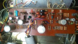
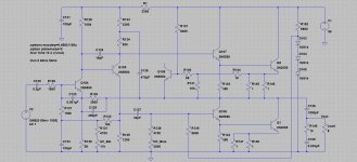
The problem I have is that my power amp board does not appear to be matching the schematics that are available online. For example, in my board C121 does not have its symmetrical for the right channel C221 and it's a 220uF cap instead of 100uF; C128 and 228 I guess are not on the board and have been changed in value (2200uF instead of 1000, and mounted on the front frame), and the overall layout of the components is quite different. However, my board appears to be the same of other units of which I found pictures online.
As I am learning electronics and troubleshooting, not having the right schematics makes all much more difficult. Does anyone happen to have the right schematics, or know what changes were made?
As for the problems, I found on the power board two burnt resistors, the same ones as in this article. Replacing them did not solve the issues the amp has.
With a 1V peak to peak 1kHz signal, the output right channel shows at max volume a very noisy 400mV peak to peak sinewave. I can record that signal with my signal tracer as well, very very weak.
The left channel does not show anything apart from a weird 100 hZ oscillation regardless of the position of the volume knob.
The voltages on the left channel across Q104, Q105 and Q106 do not match the schematics at all: for example Q106 shows around 52V at all the terminals (C, B, E), Q105 shows 33V instead of 30.2 at the collector, and 26.6 at both the emitter and base, and Q104 shows 27.7V at the base. Not being sure what the right circuit is, I don't really know where those values come from.
I found a Sony TA-1010 for almost nothing, the person who sold it told me the left channel had a loud hum and the left channel was OK.
I got it home, cleaned it thoroughly, and started checking what's wrong.
The preamp section and the tone control section appear to be working OK, with all the voltages matching the schematics.
The problem I have is that my power amp board does not appear to be matching the schematics that are available online. For example, in my board C121 does not have its symmetrical for the right channel C221 and it's a 220uF cap instead of 100uF; C128 and 228 I guess are not on the board and have been changed in value (2200uF instead of 1000, and mounted on the front frame), and the overall layout of the components is quite different. However, my board appears to be the same of other units of which I found pictures online.
As I am learning electronics and troubleshooting, not having the right schematics makes all much more difficult. Does anyone happen to have the right schematics, or know what changes were made?
As for the problems, I found on the power board two burnt resistors, the same ones as in this article. Replacing them did not solve the issues the amp has.
With a 1V peak to peak 1kHz signal, the output right channel shows at max volume a very noisy 400mV peak to peak sinewave. I can record that signal with my signal tracer as well, very very weak.
The left channel does not show anything apart from a weird 100 hZ oscillation regardless of the position of the volume knob.
The voltages on the left channel across Q104, Q105 and Q106 do not match the schematics at all: for example Q106 shows around 52V at all the terminals (C, B, E), Q105 shows 33V instead of 30.2 at the collector, and 26.6 at both the emitter and base, and Q104 shows 27.7V at the base. Not being sure what the right circuit is, I don't really know where those values come from.
Attachments
thats an old one for sure, one of the first solid state amps by appearance.
schematic may be available online. looking at pictures there appear to be several large trimpots that probably are bad and should be replaced. carefully remove them and test the resistance accross the outer terminals and replace with similar value. New ones are much smaller and may need jumper wires to each pot.
check all voltage regulator outputs and amp transistors for shorts. if short found, replace the outputs and driver transistors.
This amp has a very unusual power amp section in that all the active devices are NPN.
If you are finding differences in component values between left and right channels then I would say that is a certain sign the amp has been worked on before by other persons unknown.
You need to use a 'bulb tester' while working on this in order to limit current and prevent damage.
It would certainly make an interesting project to restore.
It does not seem that anyone has done any work on the amp before.
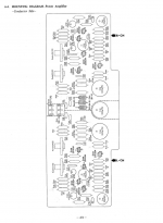
The layout of the board seem just different, I guess mine is a later version? Pictures online show a board that look like the one I have, and not the one in the schematics.
The layout of the board seem just different, I guess mine is a later version? Pictures online show a board that look like the one I have, and not the one in the schematics.
Attachments
Interesting. Yes it does look like different in layout.
Although it makes things more difficult, it should still be possible to fault find on this as long as you take your time and are careful.
Although it makes things more difficult, it should still be possible to fault find on this as long as you take your time and are careful.
So, after some testing it seems that one of the two output transistors (Q109) in the left channel is completely open. Emitter, collector and base all show around 54V. This sets the collector of Q110 at 54V. Sure enough, the resistances between the pins of Q109 are in the 10 Ohm range.
I ordered some replacements and once they come in, I will check what other issues there are.
All the voltages in the right channel check OK, it's really a mystery why there is almost no sound from the right channel.
The schematics show the signal voltages in dBm at the various stages, but I have no clue how to test them. Does anyone have any advice for that?
Thanks again
With the same voltage on all 3 pins it will be short circuit rather than open. Also check the 1 ohm emitter resistors on both output transistors.
An oscilloscope is the correct tool for fault finding and tracing signals and levels. You should be able to pick up a clean signal on C120 and that should be amplified by the power amp section... which appears to have an extremely high gain by modern standards.
Sony always give dbm levels but they are of little use for faultfinding. A line input of around 150mv rms should be enough to fully drive the amplifier up to clipping.
And don't forget to use a bulb tester at all times, otherwise your replacement transistors could go the same way.
I'd also include some electrolytic cap health checks if possible - or just change / upgrade them, they're almost 40 years old.
If you're in UK, the 100Hz 'oscillation' sounds like ripple on the power supply.
If you're in UK, the 100Hz 'oscillation' sounds like ripple on the power supply.
What's surprising about the 100Hz oscillation is that it shows only in the left channel and not in the right one.
I was already planning to replace all the electrolytic caps, still waiting for my order to be delivered.
I was already planning to replace all the electrolytic caps, still waiting for my order to be delivered.
You said Q109 is shorted - so 100Hz goes straight through the shorted C-E to the output.
yeah, that makes sense, I didn't see that.
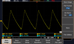
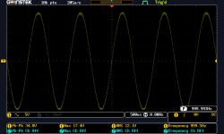
Here is the output on the oscilloscope from the right channel.
The signal at the output of the preamplifier is so weak that the oscilloscope registers mostly noise. I can however hear it very weakly using a signal tracer maxed out in volume.
At full volume on the amp, I get an output at the speaker terminals of 120mV pk to pk.
My input is a crazy 2V 1kHz sine wave, the output frequency is maintained at 1kHz
Attachments
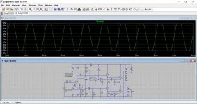
The lack of PNP devices makes this such an unusual amplifier that I decided to simulate it. (protection transistor disabled as I find it to aggressive. Probably differences in modern semi turn on volts... the resistor values would need tweaking)
I've attached the .asc file. Someone may find it useful at some point.
I've attached the .asc file. Someone may find it useful at some point.
Attachments
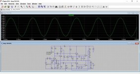
The lack of PNP devices makes this such an unusual amplifier that I decided to simulate it.
wow, thanks for doing that! 🙂
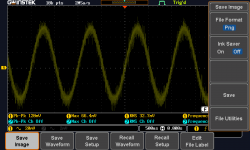
Update: tracing signals on the right channel made me get to the conclusion that the amplifier works, and the problem is just a malfunctioning source switch. Bypassing the switch completely, I managed to get a nice signal at the output speakers, that starts clipping at about 13.5W instead of the 15 that the amplifier is rated at.
Attachments


I finally got some time to have a better look at what could have gone wrong in the amplifier. Funny thing, of all the transistors in the circuit the only one that didn't fail was the one in the protection. I don't really know exactly what, but something catastrophic happened. Luckily Q108 was shorted from C-E, and open in the B-E junction, so one of the two output transistors was still functional. I replaced the broken transistors with some 2SC1815, for both the 2SC632 and 2SC634.
I matched the Q107 and Q108 with a curve tracer, and replaced all the electrolytic caps.
After adjusting the DC bias, it works like a charm, it outputs about 21.4W from the left channel (the one with the new 2SC1815), and 18.4W from the channel with the old transistors.
It would be interesting to know what made the left channel fail so badly.
Even if the layout of the board is different than in the manual, the circuit is the exact same. The only difference I found was C121, 220uF in the board and 100uF in the schematics. I don't think anyone replaced it, it should have come out of the factory that way.
It sounds quite nice, not as annoyingly sharp like e.g. a Rotel RA412, quite relaxed, with a surprising smoothness and presence of bass and good stereo separation. It don't find it very engaging though.
Attachments

 well done, that's excellent news. Direct coupled stages can always do plenty of damage when something fails... if you look at the circuit you will see there are some pretty low 'possible' impedance paths available... depending on exactly what went pop first of course.
- Status
- Not open for further replies.
- Home
- Amplifiers
- Solid State
- Sony TA-1010 restoration