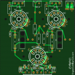
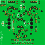
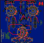
Figured I would share my latest larf with you guys. I've been playing with EasyEDA (online PCB design software) for various projects, and decided to knock together a little EL84 SE board. It takes a single noval driver tube (12AX7, 6N2P, 6N1P, 6CG7,6DJ8, etc) and can use UL, triode, or pentode mode output connection. The driver stage can be biased with a resistor (with or wiithout capacitor bypass) or an LED, and either choice allows the use of global negative feedback as well. I put some ventilation holes under the output tube cathodes to keep things cool too. Should be a handy little board for simple builds. It's got a simple CRC onboard as it assumes some external PSU filtering (likely a rectifier tube and a choke, or one of my mosfet boards I'm working up) to keep things simple. The bottom layer has a ground plane. Once I get it to a point where I think it's basically done I'll replace the output sockets with octals to allow use with 6V6 and 6L6 types too. So far the board is just at 100mm square, which keeps it cheap from most places (like JLCPCB 🙂)
Ignore the obviously nonsense parts values, I'll change those soon, as well as fix a few ground connections that are missing.
I've got a pile of 6N1P, 6P14P and 6P6S on hand, so I wanted a few boards to have something repeatable for all the builds I do for folks, as point-to-point gets tiring when you build a dozen or so of the same basic amplifiers and circuits each year 😉
Attachments
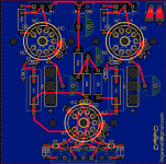
Technically, it seems like it could have been a one-sided board (at least with the traces, not the ground-plane). The connection between R24 and R25 on the ground-plane side could have been fished thru the valve pins 7 and 8 of U1, and the connection from pin 8 of U₁ to CK anode likewise could have been fished thru conveniently enough. For reasons that are very probably “just personal”, I like to achieve 1 sided boards where at all reasonable (not just where possible!)
Otherwise, looks good. I like the filament power-by-twisted-pair concept. I've always distrusted doing that part "on the board".
Just saying,
GoatGuy
Otherwise, looks good. I like the filament power-by-twisted-pair concept. I've always distrusted doing that part "on the board".
Just saying,
GoatGuy
Thanks for taking a look!
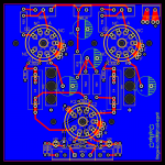
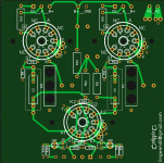
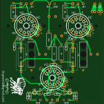
I threw those traces up on top, makes more sense, that way we keep the small signal stuff on top of the ground plane, how's this look?
Hmmm, I don't even know what to call this thing. Every simple swooky circuit needs a pretentious name! Gotta start looking up lists of obscure seldom-used words to find one that rolls off the tongue just right.
Attachments
Last edited:
I've been playing with EasyEDA (online PCB design software) for various projects, and decided to knock together a little EL84 SE board.
Make sure you have enough HV isolation between the pads and the ground plane.
Yeah I'm looking into how to increase the clearance on the higher voltage bits specifically, I can't find an option per pad to do so. I may need to manually remove copper pour near them somehow. As it is now I've got .75 mm globally, but I'd like at least 1~1.25 mm on the supply and plate voltages.
I'm looking into how to increase the clearance on the higher voltage bits
specifically, I can't find an option per pad to do so.
I imagine you'd have to enlarge the particular HV pad before doing the copper pour.
Then afterward, shrink it back down.
how about these...Every simple swooky circuit needs a pretentious name! Gotta start looking up lists of obscure seldom-used words to find one that rolls off the tongue just right.
Elfin, Bantam, WattWallop, MiniMight
Regds.
Lingwendil, how did you design your tube socket layout in that EasyEDA software?
Or is there some library available for tube sockets?
Or is there some library available for tube sockets?
There are libraries available that are user submitted, I'll try and copy-paste the description from the listing in a bit. I've successfully used them on the flea boards, and they fit well with the "usual" ceramic sockets that are so widely available.
I made my own multi-footprint for the coupling capacitor so that both axial lead and box types can be used, I'll try to submit that to the library today if I can.
Next phase of work on the PCBs is to manually increase the pad-to-copper clearance for the ground plane around the supply voltage and anode connections. There isn't a way that I know of to set up individual nets with higher clearance, maybe if I edit the parts outlines with a keep-out area?
There are literally dozens of appropriate socket outlines in the user contributed section of the library, most are "9 PIN TUBE SOCKET" in the listing. I suggest you print out a copy of them to verify they are correct before committing to a design. I wish I had a better lead for you 🙂 Maybe I'll save a clone unde my username to make it easier to refer to later.
If you export the board as a PDF and set up your printer correct, you can print out a copy in real-size to verify everything fits. Handy.
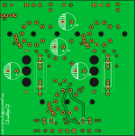
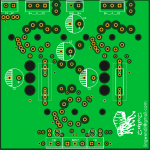
More work on the PCB- I added some large keepout areas (and still working on it, notice the lack of them on the screen resistors) on the ground plane around the higher voltage pins. UL requirements state that .8mm is good for up to 500V if both connections are coated, but I increased this around the higher stuff just to be safe. Should be good to go!
I've changed the ground pads to "solid" rather than "spoke" connection, also (not pictured) due to the adjacent connections making for poor connection as can be seen on some screenshots. This isn't likely to cause any issues during construction, but should prove for a better connection. As of now, all signal traces are on top of the board for shielding with the bottom ground plane.
Minr tweaking is next, and I still need to draw up a legible schematic, but be assured that this is definitely pretty straightforward. Should be useful for basic builds and textbook operating conditions, with a little room for feedback and different driver biasing. Nice and simple.
If you export the board as a PDF and set up your printer correct, you can print out a copy in real-size to verify everything fits. Handy.
More work on the PCB- I added some large keepout areas (and still working on it, notice the lack of them on the screen resistors) on the ground plane around the higher voltage pins. UL requirements state that .8mm is good for up to 500V if both connections are coated, but I increased this around the higher stuff just to be safe. Should be good to go!
I've changed the ground pads to "solid" rather than "spoke" connection, also (not pictured) due to the adjacent connections making for poor connection as can be seen on some screenshots. This isn't likely to cause any issues during construction, but should prove for a better connection. As of now, all signal traces are on top of the board for shielding with the bottom ground plane.
Minr tweaking is next, and I still need to draw up a legible schematic, but be assured that this is definitely pretty straightforward. Should be useful for basic builds and textbook operating conditions, with a little room for feedback and different driver biasing. Nice and simple.
Attachments
Last edited:
Minor tweaking is next, and I still need to draw up a legible schematic, but be assured that this is definitely pretty straightforward. Should be useful for basic builds and textbook operating conditions, with a little room for feedback and different driver biasing. Nice and simple.
Thanks! Lurking and reading here.....🙂
Just my two cents, I'd put the signal traces on the bottom and the ground plane on the top. I have never trusted plated through holes.
If all of your signal traces are on the bottom you know that there will be no thru-hole connection problems.
If all of your signal traces are on the bottom you know that there will be no thru-hole connection problems.
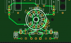
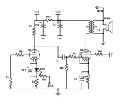
Ok, here's a schematic. The parts names are not correct on the board yet, as I'm still working on it, but I think this is the final designations for the schematic. Since this is a universal board I haven't listed parts values, since it's a little application dependent. I'll try to work some loadouts up later. The cathode of the gain stage looks a little silly but it's drawn that way to show how the board is laid out easier, I'm drawing this up in tandem with the push-pull board design I'm working on, so kept the same idea here for ease of use, and will share many of the same parts values for the front end (originally used on my Flea Amplifier as well, it's easier for me to keep track)
The board assumes an offboard power supply of your choice (my mosfet board would be useful here) however it features a basic CRC filter on board for the input/splitter stage to help out if needed, and has provision for two separate connections for two separate supply voltages to feed the input/splitter and output tubes separately if so desired.
Basically, it works as follows-
For the input stage-
-Capacitor bypassed resistor, populate CK1, and a resistor will go in the LED1 postion, standing vertically, jumper out R4, leave R9 open, no global negative feedback
--Same as above, with added R4/R9 resistor combination for negative feedback
-LED bias, populate LED1 position, leave off the CK1 capacitor position, jumper out R4, leave R9 open, no global negative feedback
--Same as above, with added R4/R9 resistor combination for negative feedback
-Unbypassed cathode resistor, jumper out either CK1 or LED1, populate R4, do not populate R9, no global negative feedback
-Same as above, with added R9 for negative feedback (this is my preferred use!)
For the output stage screens-
-Triode mode, connect R8 to the anode of the respective tube (additional pads are provided) rather than to the output connector. populate the output terminal with a 2POS terminal (or a 3POS for later experimentation)
-Ultralinear mode, populate R8 as shown on the board. Populate output terminal block with 3POS terminal. Connect off-board as shown on chosen transformer wiring diagram.
-Pentode mode, Connect as above for ultralinear mode, and bring leads from output terminal to external (adjustable, if possible) power supply. (this is my preferred use!)
Attachments
Last edited:
Ok, here's a schematic.
You need a grid #1 resistor to ground for V3.
Had a quick look at the schematic : after applying the NFB no sign of oscillations or ringing?
Last edited:
With the handful of amplifiers that I have built using this scheme I've never had an issue, but it assumes quality iron. Worse case put a capacitor across the feedback resistor as needed. I haven't included one on the board or schematic as it may need to be chosen by the builder at construction/testing.
Easy enough to do the initial testing with clip leads. If anybody has suggestions on parts outlines for caps to fit on the PCB I'm all ears, but there are so many types and sizes I wasn't sure of a good "one size fits all" value or outline.
Easy enough to do the initial testing with clip leads. If anybody has suggestions on parts outlines for caps to fit on the PCB I'm all ears, but there are so many types and sizes I wasn't sure of a good "one size fits all" value or outline.
Is this a Flea amplifier too? I suppose an EL84 Triode SE qualifies, does it not? I also suppose that most buildouts would qualify as flea power with this board.
Well, either way, this board seems to have ended up with fleas 🙂
Parts names are now accurate to the schematic too. I'm thinking the overall idea is pretty much finished. I've got my ear open for any further suggestions, but I've incorporated everything I wanted so far.
For anybody that is curious, the Flea is from Openclipart.org, and has an unlimited public/commercial use license. Handy resource 🙂
What shall we do for a name? the FleaSE? FrugalSE? Hmmm.
FleaSE does have a certain ring to it.
Attachments
- Status
- Not open for further replies.
- Home
- Amplifiers
- Tubes / Valves
- Some PCB design practice, an SE board is born!