Any ideas how to make car SMPS Current protection? How to make negative rail protection?
An externally hosted image should be here but it was not working when we last tested it.
Attachments
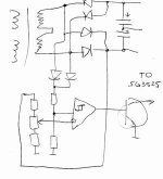
I drawed caps backeards  ups.. I want to limit output current. For example - to turn of sg3525 at 8 Amperes in rail or maby short circuit protection. I want to protect the smps from overload. I had made protection via adding transformers in primari side, but it is dificult to make them, and constructive place them somewhere..
ups.. I want to limit output current. For example - to turn of sg3525 at 8 Amperes in rail or maby short circuit protection. I want to protect the smps from overload. I had made protection via adding transformers in primari side, but it is dificult to make them, and constructive place them somewhere..Attachments
And why don't you sense voltage drop across the MOSFETs in the primary side during the on period? The own switching devices can act as sense resistors for free, all what you have to do is to take the drain voltage through a resistor and switch it to ground while the device is off (some blanking delay is required after turn-on and before turn-off). Then, a comparator feeding the shutdown input of the SG3525 produces a nice pulse-by-pulse current limiting (remember to add slope compensation if you use regulation).
Furthermore, as Rds-on increases with temperature, the current limiting threshold will be lowered as the transistors get hotter.
Furthermore, as Rds-on increases with temperature, the current limiting threshold will be lowered as the transistors get hotter.
Check that web:
http://www.bobblick.com/techref/projects/mp3book/mp3book2/mp3book2.html
And the two last pages of that thread:
http://www.diyaudio.com/forums/showthread.php?s=&threadid=74800&perpage=10&pagenumber=2
I have tried it with quite success in a 12V transformer driven frluorescent dimmer, altough it requires playing with component values around the transistor that shunts the drain reference to ground during off-time, and adding some zener clamps is quite useful.
If for example there is transformer sensing employed could the grounds of the two fets be tied together than ran thru one sense transformer? or would that be very in-accurate?
Note that this thread is not about sense transformers, but about transformerless sensing 🙂
Anyway, transformers require a symmetrical Volts*seconds/turn product to be applied on the core to prevent saturation (if you applied 1V per turn during 10us, then you have to apply -1V during another 10us to continue normal operation). However, current sense signals are usually unipolar pulses, and when they are bipolar then tend to be not perfectly symmetrical, so two transformers are required in order to use one while the other "resets".
You'll have to understand transformers first... Also, people usually has a lot of trouble understanding current transformers.
Concerning the volts*seconds/turn concept, note that the core doesn't mind at all about the total number of turns used, only the voltage-per-turn ratio matters (and that same voltage is forced to appear across every turn due to magnetic coupling).
I have successfully designed an overcurrent protection without resistors, based on mosfet Rds(on) for my Class-D amplifiers, but I want to raise a question:
If you try to apply that principle to a CAR SMPS, where mosfet losses are very low (typically in the order of 5 mohm when parallelling a couple of them), you will get such a small sense voltage even at high currents that perhaps it would be impractical to detect them (we are talking about 250mV for 50A primary current) without false-triggering due to noise spikes (or being too slow if it is heavily lowpass filtered)
I don't like the sense resistors solution either, due to increased losses, size and PCB routing inconvenience, so the only practical solution I can think of is the use of a current sense transformer. However, making a CS transformer for such high currents (say, 50A) is not easy and even difficult to find in commercial catalogues.
What do you think of this?
Careful design and layout allows to obtain quite clean 250mV current sense signals. I'm also working in class D stuff now, and I'm successfully using 0.020 ohm shunts.
Note that any class D circuit is inherently much more noisier than any push-pull car SMPS due to direct switching across conducting diodes.
Note that any class D circuit is inherently much more noisier than any push-pull car SMPS due to direct switching across conducting diodes.
I've used a small piece of copper wire and connected sense wires on each end for voltage drop detection. I twisted them together and around the positive supply wire. I like to detect the supply current to the power transformer. I find breaking the ground connection to the MOSFET sources inconvenient in terms of part layout.
Eva!
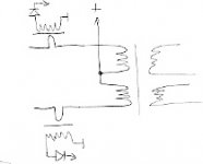
How "clean" is this waveform?
I measured this waveform after an R-C low-pass filter, on my SMPS.
the current sense were a couple of 4.7R/1206 resistors. After them, there was an R-C low-pass-filter, made from 1K and 470pF.
(Ths circuit was a full bridge SMPS)
How "clean" is this waveform?
An externally hosted image should be here but it was not working when we last tested it.
I measured this waveform after an R-C low-pass filter, on my SMPS.
the current sense were a couple of 4.7R/1206 resistors. After them, there was an R-C low-pass-filter, made from 1K and 470pF.
(Ths circuit was a full bridge SMPS)
It seems quite clean to me. For average current control it would be absolutely fine. For peak current control or limiting it may cause false triggering. However, these traces of ringing seen (at switch turn on??) are probably common mode noise that is appearing on your oscilloscope but is not being seen by components placed locally near the sense circuit.
BTW: You may try to optimize your circuit to make it produce less common-mode ringing, maybe by slowing down switch turn-on.
Also, a properly sized RC filter network is almost mandatory and does not make any harm because it compensates for sense element inductance and provides a true current waveform reference without steps on transients. A second order filter would be required to actually get a current reference with its high frequency components rolled off.
Hello!
Unfortunatelly I couldn't measure the waveform directly at the "CS" pin of the PWM-controller IC (UCC 2808), becouse the circuits makes strange noise,when I touch the CS pin with the 'scope probe. The sound is like, when the feedback is unstable.
Here's the layout of that circuit:
http://sziget.mine.nu/~danko/aramkor/testbed/14/gkrellShoot_01-28-06_142456.gif
The two "X" mark the place, where I measured this waveform:
Near the "-" pin of the diode-bridge, there's the RC-low-pass-filter, I took the previously posted picture at there.
Unfortunatelly I couldn't measure the waveform directly at the "CS" pin of the PWM-controller IC (UCC 2808), becouse the circuits makes strange noise,when I touch the CS pin with the 'scope probe. The sound is like, when the feedback is unstable.
Here's the layout of that circuit:
http://sziget.mine.nu/~danko/aramkor/testbed/14/gkrellShoot_01-28-06_142456.gif
The two "X" mark the place, where I measured this waveform:
An externally hosted image should be here but it was not working when we last tested it.
I don't remember the volt/div of the picture... 🙁
Near the "-" pin of the diode-bridge, there's the RC-low-pass-filter, I took the previously posted picture at there.
You will probably get cleaner waveforms by removing anything in parallel with main electrolytic filter capacitors, it may not seem too obvious but the lower the supply impedance at RF, the more spikes and EMI produced. Also, you should employ R plus R and D in parallel in series with the gates in order to get a fast turn-off dominated by capacitances and an intentionally slowed down turn-on. That will also produce cleaner waveforms and far less EMI.
Also, you should place the RC filter near the control IC and referenced to its ground in order to get a cleaner signal into the comparator.
Note that you have one decoupling capacitor from supply to drain/emitter on each gate drive IC, while the positive supply rail going to both ICs is just paralleled. It may be useful to add series resistors or inductors to get the supplies mutually decoupled, otherwise drain/emitter currents will also tend to flow in them.
BTW: You are very lucky if you haven't already blown a dozen of those gate drive ICs without external buffers that look like IR2112.
With this circuit, I was lucky 😉
I haven't burned a single semiconductor! I think, this was a miracle... 🙂
This circuit was just an experiment, I have disassembled it. But I will try this R+R-D thing, series with the GATE. (thoose TO247 package devices were IRF74)
You write, that I may decouple each gate-driver IC. You think something, like this?
What kind of external buffer do did think, when you wrote this?
I'm using IR2113.
By using an external buffer, you was thinking something, like this?
http://users.tkk.fi/~jwagner/electr/subw-digiamp/MOSFEThalfbridge-sch.gif
I haven't burned a single semiconductor! I think, this was a miracle... 🙂
This circuit was just an experiment, I have disassembled it. But I will try this R+R-D thing, series with the GATE. (thoose TO247 package devices were IRF74)
You write, that I may decouple each gate-driver IC. You think something, like this?
An externally hosted image should be here but it was not working when we last tested it.
What kind of external buffer do did think, when you wrote this?
You are very lucky if you haven't already blown a dozen of those gate drive ICs without external buffers that look like IR2112.
I'm using IR2113.
By using an external buffer, you was thinking something, like this?
http://users.tkk.fi/~jwagner/electr/subw-digiamp/MOSFEThalfbridge-sch.gif
I mean that a lot of people complains about IR2110/2113 unexpectedly blowing in some applications, but if yours survive, then continue using them.
I prefer IR2112 (+-200mA) with a pair of external PNP/NPN buffer transistors for experimentation, it uses more space but it's cheaper when it fails 😀
I prefer IR2112 (+-200mA) with a pair of external PNP/NPN buffer transistors for experimentation, it uses more space but it's cheaper when it fails 😀
I have used some IRF7343 dual N/P channel MOSFETs even on experimental circuits in which the MOSFETs kept blowing without blowing my IR2113. I have used that method in a project which has been operating for almost two years continuously, too. The 27 ohm resistor may be a different value, depending on the circuit.
ImageShack
An externally hosted image should be here but it was not working when we last tested it.
ImageShack
Boosting an IR2112 with bipolar transistors is a good idea, I think I will try it sometime. 🙂
In this experiment all the semiconductors survived my tortures, but in other circuits I fried plenty of IR2113s 🙁
Thanks you opinions Eva! 🙂
In this experiment all the semiconductors survived my tortures, but in other circuits I fried plenty of IR2113s 🙁
Thanks you opinions Eva! 🙂
- Status
- Not open for further replies.
- Home
- Amplifiers
- Power Supplies
- SMPS Current protection