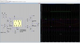
I have attached a picture of the schematic of a very simple Sigma Delta class D amplifier with some diagrams.
The circuit consists of a Sigma Delta pulse width converter based on a NE555, a voltage controlled current source which influences the charging current of the capacitor of the converter and the output stage. I have left the low pass filter, because most of the speakers cannot follow the modulation frequency of about 200 kHz.
What do you think about this circuit? Which means for improvement would you suggest, which doesn't make the circuit significantly more complex. Do you see any means for a less complicated circuit?
Attachments
Shoot-through will almost certainly happen in that circuit. Perhaps add diodes to speed up switch-off of each MOSFET and increase the parallel resistors to slow-down switch-on of the opposite one.
Also replace the 555 with a 7555, usually a wise move given the decoupling nightmare of the original 555.
Also replace the 555 with a 7555, usually a wise move given the decoupling nightmare of the original 555.
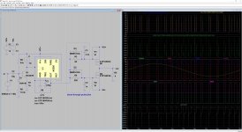
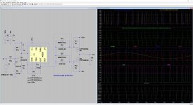
I have still improved the shoot through protection and attached a low pass filter behind the output. The peek power across the output transistors is a little bit higher but the average power is reduced significantly.
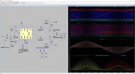
The diagrams are for 1 kHz. The Sigma Delta modulation is very nice visible in the voltage diagram.
The diagrams are for 1 kHz. The Sigma Delta modulation is very nice visible in the voltage diagram.
Attachments
The NE555 has not much output current capability (200mA) you would be better off using a dedicated gate driver IC in addition to it. That could also include dead time insertion logic or you can do this using a few logic gates and RC delays. This would also allow you to use two NMOS transistors which have better performance than PMOS as it would implement the required level shifting and drive voltage generation for the high side device.
http://www.ti.com/power-management/gate-drivers/half-bridge-drivers/products.html
http://www.ti.com/power-management/gate-drivers/half-bridge-drivers/products.html
- Status
- Not open for further replies.