The HP-1000 is a stereo integrated amp made in Chicago, IL around 1977 by the original Sherwood company. It's rated at 60wpc with 0.1% THD.
I'm planning to restore one and get it closer to 0.001% THD, by replacing the power amp with a variant of ostripper's Wolverine done on a custom PCB.
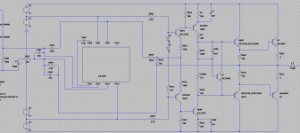
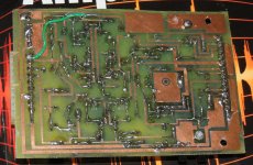
From the factory, the power amp circuit uses a CA3100 op-amp as the front end. It has a sort of push-pull VAS and conventional output stage. The attachment here is the factory amp.
EDIT: the transistor types in this spice deck aren't accurate, they are modern transistors for which models happen to exist.
I'm planning to restore one and get it closer to 0.001% THD, by replacing the power amp with a variant of ostripper's Wolverine done on a custom PCB.
From the factory, the power amp circuit uses a CA3100 op-amp as the front end. It has a sort of push-pull VAS and conventional output stage. The attachment here is the factory amp.
EDIT: the transistor types in this spice deck aren't accurate, they are modern transistors for which models happen to exist.
Attachments
Last edited:
My first idea was to modify the factory compensation scheme to incorporate TMC. A lot of Lin amps can be converted to TMC with just a few added components, and the distortion floor drops 20db. TMC is magic. But this is not a Lin amp, and I couldn't figure out how to TMC it.
The factory Sherwood amp doesn't exactly have a typical Miller cap. A typical Miller cap would have one terminal on a voltage that swings with the signal (the VAS output, usually) and the other terminal on a current-sensitive node whose voltage doesn't swing much (the long-tailed pair output, usually.)
The only cap here that may fit that description is C604. This is a guess; I have a fuzzy understanding of what's going on inside the CA3100. You can't just replace that cap with a TMC network because the VAS is inverting, so you can't just substitute the VAS output for pin 8 on the opamp.
A typical modern opamp is no help. The long-tailed pair is hidden within the IC. External nodes are voltage-referenced, none are current-sensitive.
I guess is there are good reasons not to build a power amp around an opamp. The factory PCB is very much oriented around this opamp, and quite dense with components, so my guess is that the factory PCB is also a dead end.
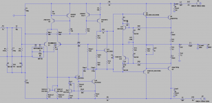
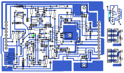
Here's the Wolverine clone schematic and new PCB. The two rows of oversized pads at the right and left edges are for the connectors which I'm planning to transplant from the factory PCB.
This is my first attempt at a custom PCB. I was too cheap to pay for Eagle so I used the GNU 'pcb' program on linux (google for 'geda pcb'.) That may or may not have been a wise decision; it took longer than I thought to lay this out. How long should it take to lay out a board of this size?
This is my first attempt at a custom PCB. I was too cheap to pay for Eagle so I used the GNU 'pcb' program on linux (google for 'geda pcb'.) That may or may not have been a wise decision; it took longer than I thought to lay this out. How long should it take to lay out a board of this size?
Attachments

The amplifier boards are built, populated, and they run.
I recapped the preamp with C0G's and replaced the TBA231 opamps with OPA1612's using custom adapter PCBs. There are two adapters left over, pm me if you're looking for 2 adapters that connect a TBA231 footprint to any dual SMT opamp.
I recapped the preamp with C0G's and replaced the TBA231 opamps with OPA1612's using custom adapter PCBs. There are two adapters left over, pm me if you're looking for 2 adapters that connect a TBA231 footprint to any dual SMT opamp.
Next step, real world stability testing. The Wolverine in Sherwood's chassis has gotta be unflappable.
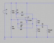
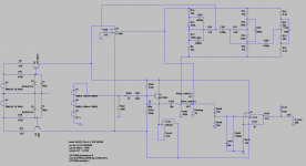
I may build the square wave generator below. Spice shows edges with rise and fall time around 15ns. That should be faster than the amp's slew rate. It should reveal any ringing, up to several MHz, and worst-case overshoot.
A stable amp should make less than 20% overshoot, that correlates to a phase margin better than 45 degrees. See figure 8 here, http://www.ti.com/lit/an/sloa020a/sloa020a.pdf
Attachments
Pics 😀
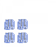
The new driver boards look sharp.
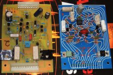
3rd pic is a comparison with an original one, or what's left of it anyway. I stole the connectors, heatsinks, and wirewound output resistors off the OEM board.
The new driver boards look sharp.
3rd pic is a comparison with an original one, or what's left of it anyway. I stole the connectors, heatsinks, and wirewound output resistors off the OEM board.
Attachments
pics!
The driver PCBs mount in the chassis with the OEM connectors and stand-offs.
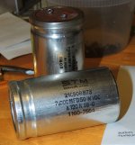
This also shows new main filter caps, they are 105 centigrade Panasonic 10,000uF sleeved in PVC pipe to fit the OEM clamp. The new caps aren't as sharp looking as the Soul-of-a-New-Machine-era originals. COMPUTER GRADE!
The driver PCBs mount in the chassis with the OEM connectors and stand-offs.
This also shows new main filter caps, they are 105 centigrade Panasonic 10,000uF sleeved in PVC pipe to fit the OEM clamp. The new caps aren't as sharp looking as the Soul-of-a-New-Machine-era originals. COMPUTER GRADE!
Attachments
pics 😵
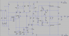
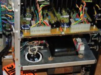
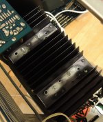
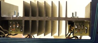
1- Far side of the heatsink where the original TO-3 devices mounted. Just nuts and bolts are there now. Some paint is sanded off to get a good electric ground.
2- Output transistor PCBs. Each has a MJW1302 or MJW3281 plus a zobel network for the power rail (that's what the ground to heatsink is for.) This keeps the power rail from looking inductive to the output's collector. There's an aluminum oxide pad beneath each device.
3- One of two preamp PCBs, the service manual calls this the "filter" board. It has the high filter, low filter, and tone defeat switches. You'll notice a lot of empty pads: Sherwood's high and low filter implementation really didn't want to produce a flat response (even with filters off) and this was not easy to fix. Long story short, I deleted a lot of cruft here and disabled the high filter and low filter functions. All other functions are unaffected, including the variable curve loudness and the tone controls which sound real good recapped with c0g's.
You'll also notice some drilled out traces on the filter board. To reduce hum and hiss at idle, I made the paths from the volume pot to the opamp inputs as short as possible and trimmed extra trace length that might act as an antenna. I also rerouted the signal-ground between volume pot output and opamp input, so that it no longer shares a trace with another ground path that carries a bunch of AC current. The circuitry between volume pot output and opamp input is critical; this signal is boosted 160x at the speaker outputs so it must be quiet to start.
Attachments
Last edited:
Here are final versions of the amp and preamp schematics, and the PCBs.
There's a mistake on the amp PCB that required an ECO. In the PCB here, the output zobel network shares a ground return path with C3, C5, and Q3 and that caused some instability. To fix that I drilled out the trace and ran a jumper (green wire on the solder-side photo above) to create an independent ground path for the output zobel.
This opamp adapter takes a TBA231 footprint and fits a standard dual SMT opamp. It also takes 2 resistors and 2 caps to provide a local filter on the supply rails; I used 100 ohms and 1uF ceramics. The adapter is not a drop-in replacement for the TBA231, it requires pin 3 on the original TBA231 footprint to be grounded. That's easy to do on any TBA231 application -- delete the compensation cap that isn't needed for any modern opamp, and jumper ground to the free pad left behind by the cap.
Attachments
- Status
- Not open for further replies.
- Home
- Amplifiers
- Solid State
- Sherwood HP-1000 restomod