Hi all,
I have been trying to diagnose a problem with my Sony DAS-702ES DAC (I have another thread on the subject). I am a seasoned hifi/AV/tech enthusiast but my knowledge of the more in-depth electronics is lacking sadly. I am hoping you can help!
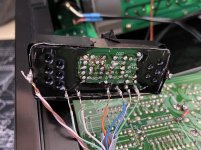
I have a problem where there is a digital static produced by the DAC which I had narrowed down to the digital board, in particular the VCO block. If I moved the block or pressed down on the board above it, the issue would stop.
I removed the VCO block and joined it to the main board by means of some wire to see if I could troubleshoot it easier.
I have pictured it attached.
It seems that, when the digital static occurs (I'm assuming lack of oscillation meaning it can't properly lock onto the SPDIF signal, or something), I can press on the black potted area on the right-hand side, to make it stop.
I have resoldered all of the (visible) solder joints from the top, but this has made no difference.
Any thoughts greatly appreciated.
Service manual for the DAC here if anyone is interested:
SONY DAS-702ES SM Service Manual download, schematics, eeprom, repair info for electronics experts
Obviously this thing is ancient now, so no spares available.
Thank you very much.
I have been trying to diagnose a problem with my Sony DAS-702ES DAC (I have another thread on the subject). I am a seasoned hifi/AV/tech enthusiast but my knowledge of the more in-depth electronics is lacking sadly. I am hoping you can help!
I have a problem where there is a digital static produced by the DAC which I had narrowed down to the digital board, in particular the VCO block. If I moved the block or pressed down on the board above it, the issue would stop.
I removed the VCO block and joined it to the main board by means of some wire to see if I could troubleshoot it easier.
I have pictured it attached.
It seems that, when the digital static occurs (I'm assuming lack of oscillation meaning it can't properly lock onto the SPDIF signal, or something), I can press on the black potted area on the right-hand side, to make it stop.
I have resoldered all of the (visible) solder joints from the top, but this has made no difference.
Any thoughts greatly appreciated.
Service manual for the DAC here if anyone is interested:
SONY DAS-702ES SM Service Manual download, schematics, eeprom, repair info for electronics experts
Obviously this thing is ancient now, so no spares available.
Thank you very much.
Attachments
When you touch the various connections and it stops, you have with your hand added extra capacitace and resistance to smooth the oscillation out. You might try to simulate your magic hand with actual small capacitances and high resistances on the most susceptable connections.
When you touch the various connections and it stops, you have with your hand added extra capacitace and resistance to smooth the oscillation out. You might try to simulate your magic hand with actual small capacitances and high resistances on the most susceptable connections.
Thank you, that's actually a very good idea.
Could you suggest any appropriate values?
🙂
How about poking it with a pencil?
I'd try to replace the PCB as my suspicion is there's a break in at least one of the tracks.
Failing that, if mechanical intervention (ie, gently bending the PCB) is required, I'd be looking at a way to permanently apply that pressure.
Chris
I'd try to replace the PCB as my suspicion is there's a break in at least one of the tracks.
Failing that, if mechanical intervention (ie, gently bending the PCB) is required, I'd be looking at a way to permanently apply that pressure.
Chris
...f I moved the block or pressed down on the board above it, the issue would stop.....
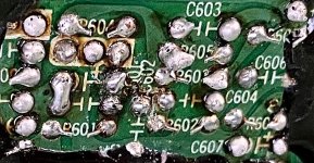
Hmmm. Those joints are still fluxy and blobby. A joint should be clean and lean so you can see "wetting". While I would start with touch-up, if no good result I would suck/wick/bang 99% of the solder off, inspect the surfaces, flux as needed, then do solder joints so lean they can be visually inspected.
13 Common PCB Soldering Problems to Avoid - Latest open tech from seeed studio
PCB Soldering Common Problems And Reparing Way | Leadsintec
Attachments
Last edited:
I like to apply flux-off to clean the flux after soldering and then a brush like polishing shoes. Sometimes I apply a coat of PCB spray polyurethane varnish.
Putting pressure on one part of the board, might actually be flexing a different part of the board.
I would remove all potting then desolder and resolder very slowly to avoid heat damage.
Then clean it to reveal any soldering issues.
And sorry, but I see a lot of very suspect joints in that pic.
I would remove all potting then desolder and resolder very slowly to avoid heat damage.
Then clean it to reveal any soldering issues.
And sorry, but I see a lot of very suspect joints in that pic.
- Home
- General Interest
- Everything Else
- Repairing suspected faulty board covered in potting compound?