Problem at drivers, output devices... (transistors has broken down).
I'm talking about pure simulation. Not actual devices.
Input currents to the input transistors - Q2 and Q3. Also, Unbalnced currents between the two transistors. I presume you are toakking about small (20 to 200 mV offsets.) Feed back will set the current through Q3 to about 1.5 mA (enough to cause q( to turn on. The current source supplies about 6mA, so Q2 will have about 4.5 mA collector current, so there will be differences (but very small) in Vbe for the input pair. Bigger different will be because of the base currents for the base pair. Calculate base currents, and then figure out the voltages across r4 and R6, then figre out how much offset to cancel them through R8 (It's why most amps have a capacitor on the feedback resistor going to ground, and try to keep the other feedback resistor equal to the input resistor)(Assume base voltages are about the same.) My 2 cents
Addenda - rough numbers - assuming hfe of 300 - base current on input transistor Q3 is about 15 uA - means input is at -150 mV. For the output side to be -150mV means output has to be -1.5 volts. What kind of numbers are you getting with sim?
Addenda - rough numbers - assuming hfe of 300 - base current on input transistor Q3 is about 15 uA - means input is at -150 mV. For the output side to be -150mV means output has to be -1.5 volts. What kind of numbers are you getting with sim?
Last edited:
The input pair should be a pair of matched transistors. In simulation the devices are identical, unless you deliberately make them different.
Now you need to tell the simulator what operating conditions need to be applied such that the voltages and the currents imposed on the input pair are identical.
Once you have done that you will find that the voltage on the bases of the two input transistors is identical.
That is equivalent to setting output offset to zero. The simulator will let you do that precisely if you have set up conditions as para2.
As an experiment, you can now tell the simulator to change one component value and see what effect that one component value change has on the output offset. Now try every component value around the input stage. you will quickly find which have the biggest effect and which have precisely NO EFFECT on the output offset.
DC offset
First.
In "pure" simulation You using a models. There are different models for NPN and PNP devices. No symmetry at all.
Second.
By very nature of this kind "huge feedback" amps. If You use an feedback loop without capacitor, circuit is completely sensitive for proper tuning. Its coming directly from theory of transistor operation, theory of amplifiers - electronic theory. DC operating point should be then setted properly. Maybe you noted that circuits simulated by DIY Friends have a lot of strange values like ( 1,473 OHM resistors ) instead of potentiometers used in real world.
Third.
Simulation do not showing You an thermal problems, practical realisation problems like an added inuctances, capacitances etc.
Summary:
Simulators like a P-spice are really exact with electronic theory, and showing you how and where you have to tune a circuit.
Little experiment - try to measure in P-spice Base-emitter voltage of each transistor. Try to find an DC offset with different and without load.
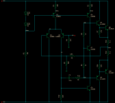
I'm viewing this on tiny screen but you seem to have 47k and 4.5k input resistors with 500 ohm return. AC couple the 500 ohm and make the other two equal.
^^^ What he said ^^^
and, is your input open circuit as shown, or are you simulating it with a signal generator connected? If you have a signal generator, it will have zero output impedance and this will affect the balance of the circuit. Better to AC couple it.
HTH,
Brian
and, is your input open circuit as shown, or are you simulating it with a signal generator connected? If you have a signal generator, it will have zero output impedance and this will affect the balance of the circuit. Better to AC couple it.
HTH,
Brian
- Status
- Not open for further replies.
- Home
- Amplifiers
- Solid State
- Reason for DC offset in a simple class AB amp?