Hi all,
Since a few weeks I have been busy prototyping my first power amplifier based on Douglas Self's Blameless design.
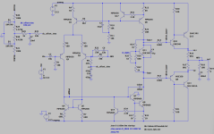
I attached the LTspice file that reflects the actual circuit (except for one of the resistors in the Vbe multiplier, because the simulation with the actual value gave a slightly too high bias voltage, whereas reality is okay).
As a first test I used a small-signal (full voltage swing, constant-current, few milli-amps) class-A output stage. This worked fine. I was able to verify the correct working of the input stage and VAS using this output stage: grounding the input resulted in near-zero volt output without dc-offset trimming, and a sine input of a few hundred millivolts gave a (relatively) clean sine output of several volts.
Currents sourced in the stages were approximately as I expected, and the voltages at various points are okay.
Then I decided to try the actual class B output stage, without any load. With great anticipation, hoping to see a nice zero volt output with grounded input, I switched on my lab supply. And got a clipping amplifier, with huge current running in the output stage.
For some time now I cannot figure out what is going on, and do not know how to continue from here.
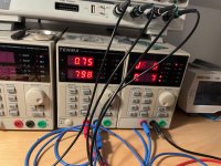
I have restricted the lab supply to different currents to see the effect of that, but mostly around 800 milli amps. This to prevent destruction of the output devices. The side effect of this is of course that the voltage rails collapse, which I think results in misbehaving small-signal stages.
To make sure that all of this was not caused by any Vbe multiplier problem I shorted the multiplier's collector to emitter, effectively removing any biasing. I rather have an amplifier with huge cross-over distortion to start with, than one that's about to apply for a job as smoke generator.
At the moment I'm short of desperate getting this thing working. What joy is awaiting me, when hearing the first tones erupting from the amplifier, after first ensuring a simple grounded input and sine input give the expected result without any load and with an 8 Ohm power resistor.
Does anyone have any clue what could be wrong or how I should proceed?
Since a few weeks I have been busy prototyping my first power amplifier based on Douglas Self's Blameless design.
I attached the LTspice file that reflects the actual circuit (except for one of the resistors in the Vbe multiplier, because the simulation with the actual value gave a slightly too high bias voltage, whereas reality is okay).
As a first test I used a small-signal (full voltage swing, constant-current, few milli-amps) class-A output stage. This worked fine. I was able to verify the correct working of the input stage and VAS using this output stage: grounding the input resulted in near-zero volt output without dc-offset trimming, and a sine input of a few hundred millivolts gave a (relatively) clean sine output of several volts.
Currents sourced in the stages were approximately as I expected, and the voltages at various points are okay.
Then I decided to try the actual class B output stage, without any load. With great anticipation, hoping to see a nice zero volt output with grounded input, I switched on my lab supply. And got a clipping amplifier, with huge current running in the output stage.
For some time now I cannot figure out what is going on, and do not know how to continue from here.
I have restricted the lab supply to different currents to see the effect of that, but mostly around 800 milli amps. This to prevent destruction of the output devices. The side effect of this is of course that the voltage rails collapse, which I think results in misbehaving small-signal stages.
To make sure that all of this was not caused by any Vbe multiplier problem I shorted the multiplier's collector to emitter, effectively removing any biasing. I rather have an amplifier with huge cross-over distortion to start with, than one that's about to apply for a job as smoke generator.
At the moment I'm short of desperate getting this thing working. What joy is awaiting me, when hearing the first tones erupting from the amplifier, after first ensuring a simple grounded input and sine input give the expected result without any load and with an 8 Ohm power resistor.
Does anyone have any clue what could be wrong or how I should proceed?
Attachments
Gain is reduced to something reasonable, say 25 db, by the Negative Feedback Loop NFB. The junction of R16 and R17 (output) has to connect to the right side of R8. Perhaps you did not realize the presence of NFB in two places means you connect them? Or perhaps there is a bad joint in the path back to base of Q1.
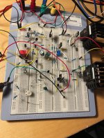
I found in Physics lab that those punch boards are hit and miss on the connections. Lab rats are presumably used harder than in the home. However, buzzing through the circuit with the "diode" scale of your dvm might find the problem.
If that does not work try connecting DVM black to speaker ground and probe with the red at various places to make sure voltages are symmetric and no transistor has 0 v or PS volts C to E.
Thanks for the reply, appreciate it!
Yes I have connected the two “NFB”s together. I chose to not draw the full connection to prevent cluttering the schematic.
When replacing the output stage with a constant-current low power output stage, the amplifier behaves well. That would rule out the bad biasing connection of Q1.
Unfortunately because of the problem, the supply rails drop to very low voltages. This prevents me from investigating the root cause by probing the voltages. I.e. the current sources stop working and the VAS transistor’s base-collector gets forward biased, resulting in large base currents (I measured 60 mA!)
By the way, what do you mean with buzzing through the circuit with the "diode" scale of your dvm ? Would that mean e.g. to check the transistors for incorrect base-collector voltages?
Just to be sure: no big mistakes with the circuit as shared? (I mean the screen shot / spice file, assuming I did not miss any wiring errors after checking this at least twenty times 🙈)
Possible oscillations due to common ground wiring or lack of phase margin. Be sure C3+R19 grounds go directly to the power supply and do not share a ground wire with C10, R1, etc.
BTW, bad idea to slave the LTP CCS off the VAS CCS since the VAS CCS can saturate on clipping and feedback to the LTP CCS. Either make the LTP master and limit the VAS CCS base current with a resistor, or use independent CCSs.
BTW, bad idea to slave the LTP CCS off the VAS CCS since the VAS CCS can saturate on clipping and feedback to the LTP CCS. Either make the LTP master and limit the VAS CCS base current with a resistor, or use independent CCSs.
One approach is to test the output stage in isolation - many signal generators can do 20V peak to peak or more, so can drive an output stage at reasonably high levels directly. Always limit current in initial testing (series resistors in the supply rails), and it helps a lot to have a tracking PSU that can raise both rails voltage in step under control.
Once you've tested the IS + VAS with a class A temporary OS, and tested the real OS separately, there's a lot more confidence they can be combined without surprizes.
Also testing at lower supply voltages and currents is less risky, with a supply that can vary both you can progress up in power in stages, rather than jumping immediately to full voltage and current!
Use 0.1uF ceramic and 47uF electrolytic in parallel for rail decoupling.
I would replace the CFP with an EF2. The protoboard has high parasitics.
Ed
I would replace the CFP with an EF2. The protoboard has high parasitics.
Ed
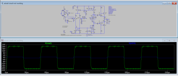
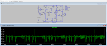
It seems to me that the OP's circuit needs a lot of work. As I am currently working on a CFP design, I downloaded the shared.asc file, fired it up in sim and injected a square wave pulse along the bases of VAS and the output node. I am posting here square wave tests at 20khz together with the result from LJMs MX50 schematic because the OPs circuit looks quite similar in design topology.
Personally I would probably run more sim tests before building a prototype for further 'scope tests, will save time.
Personally I would probably run more sim tests before building a prototype for further 'scope tests, will save time.
Attachments
Your output sziklai pairs may be oscillating (that sure has caused problems for me!). Particularly if you don't have much in the way of bypass capacitors on your supply rails. In addition to that you may need some right where the output transistors are, depends on your particular build. I have found that the parasitic inductance of a few inches of hookup wire connected to the output transistors can produce some very nasty transients, due to the combination of high current and fast edges -- V = L * di/dt. If di/dt is high, L doesn't be very big to cause problems. If nothing else, that parasitic inductance can lead to higher-than-desired gain at high frequencies, in a signal path you don't want to be present. At all.
Adding bypass capacitors right at the output devices' collectors solved my problem.
Adding bypass capacitors right at the output devices' collectors solved my problem.
Thanks all for the replies.
I will go and try fixing the ground wiring, adding decoupling capacitors and then try again with low rail voltage (+/- 6 V to start with).
If that results in a quiet amp with grounded input, I'll try a sine and gradually increase the rails to see what happens.
Glad to have found this forum, truly appreciate all help 🙂
I don’t think the blameless design has the 22p on top of the feedback resistor.
I guess it is oscillating. You can check that with an oscilloscope.
I guess it is oscillating. You can check that with an oscilloscope.
This week I got around to do some further trouble shooting.
In short: a faulty 3281 was the culprit.
First I put the output stage (with the bad transistor) on a separate breadboard. It kept running huge currents, even with grounded input.
When doing some measurements it appeared that the 3281 basically shorted its collector to emitter, resulting in the output basically stuck to the negative rail and thus very low power dissipation in the 3281. But the 1302 was running hot.
In the beginning this put me on the wrong track: I somehow concluded that something must have been wrong in the positive half of the output stage.
Boy, problems are a good source of education. I now fully understand that the 1302 was taking the full supply voltage, and quite some current, resulting in a source of heat.
After replacing both output transistors with MJE2955/3055 (had them lying around) just to see what happened, the output stage behaved as expected.
So I put some sine on it, and a (relatively) clean sine came out. Replaced the sine with some music, et voilà, some music came out.
Replaced the output transistors with the 1302 and a good 3281 still resulted in a good working output stage. No HF oscillations.
Then I felt the urge to try out the whole amplifier with the good transistors. Started with low voltage rails (+/- 8V), and a sine input gave sine output. Finally!
Then the big moment I was waiting for: hooked up some small 6 W speaker (after checking the DC offset of course, as my amplifier has no output relay and DC offset detection yet... tbd 🙂) and fed in some music. Made me happy, I heard music!
Next steps are to include the overcurrent protection, DC offset protection, output relay, output coil etc. And of course a power source.
Thanks all for the help, truly appreciate it!
It can be daunting powering up a power amp circuit for the first time. You don't want things to go phutt as soon as power is applied.
For me the first rule of power amp commissioning (well any semiconductor circuit really) is to current limit your supplies (either with lab power supply or adding series resistors for initial testing). That can prevent costly damage to components while you check all is well. I inherited some small and medium toroidal mains transformers and made myself a 0.5A switchable +/-25V <-> +/-50V supply. I used the larger ones to make a 3A +/-45V supply too.
Then I put dual adjustable current limiter and voltage regulator in a separate box. So typically I start with 25V with various current limit settings and move on to the 50V supply if all is well, then for power testing the larger supply.
Before I had the adjustable dual current limited box I would use various series resistors on the supply outputs which was more laborious. It wise to have the minimum of decoupling capacitance on the amp rails for initial testing as energy stored in those caps can be delivered without current limiting in a fault situation. 100uF per rail is pretty standard, and reasonably safe. Never include bulk filter capacitance beyond the current limiting circuit/unit!
A 4 channel 'scope is useful as you can monitor the voltage rails, the input and the ouput simultaneously.

I have an old dual 0-40V bench supply with settable current limiting and meters that gets used for this kind of work. It's saved a number of output stages over the years (along with a few other incorrectly wired circuits).Before I had the adjustable dual current limited box I would use various series resistors on the supply outputs which was more laborious. It wise to have the minimum of decoupling capacitance on the amp rails for initial testing as energy stored in those caps can be delivered without current limiting in a fault situation. 100uF per rail is pretty standard, and reasonably safe. Never include bulk filter capacitance beyond the current limiting circuit/unit!
A 4 channel 'scope is useful as you can monitor the voltage rails, the input and the ouput simultaneously.
I was fortunate to work at Tektronix in the days when their "country store" sold surplus or overstocked electronics for pennies on the dollar so managed to pick up a few items like that on the cheap. One supply is missing a handle and both are battered up some but work just fine. Those old supplies are built like brick outhouses. And correspondingly weigh a lot.
A quick search on ebay showed that similar capabilities can be had for around two hundred bucks. For that you get niceties like digital readouts and a manufacturer's warranty. Ones that also have ground and current-sense capabilities will likely cost a bit more, but personally I haven't found it necessary to use them in my bench testing setups.
The other thing I could mention is test the output stage in isolation if possible - much less to go wrong though you do need a decent signal generator with at least 10V output to be useful. That way you can be sure it doesn't oscillate and the biasing is reasonable before combining with the rest of the amp.
Similarly you can reroute the feedback take-off point to allow testing of the other parts of an amp without the output stages connected - this is considerably lower power and checks out feedback loop is working - this can be done on a breadboard for a prototype too.
Similarly you can reroute the feedback take-off point to allow testing of the other parts of an amp without the output stages connected - this is considerably lower power and checks out feedback loop is working - this can be done on a breadboard for a prototype too.
Playing with the simulation I found that the choice of MJE340/350 is a problem with 30MHz outputs. Using DB139/140 works much better for two reasons.
1. I suspect the DB139/140 are faster. Onsemi does not list the ft for MJE340/350 and I suspect it is not faster than the OPs, which is a problem because a CFP using similar speed devices is unstable because there is not one dominant pole.
2. MJE340/350 is only rated 0.5 Amps, which is not enough to drive a 15A OP. DB139/140 are rated ~3Amps.
I also note you are using MPSA06/56 in places it does not belong. They are too slow for use in the LTP etc.
And in this case C6 does not help stability. I did not check the phase margin so there may be still room for improvement.
Attachments
One more thing, make sure that your bias generator works properly. At power on let it sit for at least 2-5mins without music in it. Take a measurement of your bias current then feed some music and wait for another 2-5 mins then measure your bias current. You can repeat the process in the intervals of 5-20 mins while the amp is playing.This week I got around to do some further trouble shooting.
In short: a faulty 3281 was the culprit.
First I put the output stage (with the bad transistor) on a separate breadboard. It kept running huge currents, even with grounded input.
When doing some measurements it appeared that the 3281 basically shorted its collector to emitter, resulting in the output basically stuck to the negative rail and thus very low power dissipation in the 3281. But the 1302 was running hot.
In the beginning this put me on the wrong track: I somehow concluded that something must have been wrong in the positive half of the output stage.
Boy, problems are a good source of education. I now fully understand that the 1302 was taking the full supply voltage, and quite some current, resulting in a source of heat.
After replacing both output transistors with MJE2955/3055 (had them lying around) just to see what happened, the output stage behaved as expected.
So I put some sine on it, and a (relatively) clean sine came out. Replaced the sine with some music, et voilà, some music came out.
Replaced the output transistors with the 1302 and a good 3281 still resulted in a good working output stage. No HF oscillations.
Then I felt the urge to try out the whole amplifier with the good transistors. Started with low voltage rails (+/- 8V), and a sine input gave sine output. Finally!
Then the big moment I was waiting for: hooked up some small 6 W speaker (after checking the DC offset of course, as my amplifier has no output relay and DC offset detection yet... tbd 🙂) and fed in some music. Made me happy, I heard music!
Next steps are to include the overcurrent protection, DC offset protection, output relay, output coil etc. And of course a power source.
Thanks all for the help, truly appreciate it!
The procedure above is to simply check that your bias current is not drifting and rising from a given setting. You do not want your outputs becoming hotter and hotter while the amp is playing. I learned the procedure here at DiyAudio. 😉 Out of my four design attempts of a Sziklai amp only one worked.
Congratulations!
( PS can you share the final schematic?)
I am truly grateful for your insights and help.Playing with the simulation I found that the choice of MJE340/350 is a problem with 30MHz outputs. Using DB139/140 works much better for two reasons.
1. I suspect the DB139/140 are faster. Onsemi does not list the ft for MJE340/350 and I suspect it is not faster than the OPs, which is a problem because a CFP using similar speed devices is unstable because there is not one dominant pole.
2. MJE340/350 is only rated 0.5 Amps, which is not enough to drive a 15A OP. DB139/140 are rated ~3Amps.
I also note you are using MPSA06/56 in places it does not belong. They are too slow for use in the LTP etc.
And in this case C6 does not help stability. I did not check the phase margin so there may be still room for improvement.
I quickly changed the drivers in my simulation to DB139/140, and that basically already removes all issues I saw so far.
Regarding the MPSA06/56: I don't see an issue in my simulation with those in the input stage and VAS.
But to prevent issues in reality, and to learn a thing or two, I would love to understand the remark.
Do you mean that the MPSA06/56's Ft is too low? It's specified as 50 MHz for the 56 at -100 mA and -1 V Vce; 100 MHz for the 06 at 10 mA and 2 V Vce.
I expect that should not be an issue then?
Thanks again. Since joining this forum I am soaking up a lot of knowledge from you guys.
- Home
- Amplifiers
- Solid State
- Problem powering up first amp - any hints welcome