Hi all,
I was looking for a reasonable amplifier to build for a multi channel system. I like Bob Cordell's book and so decided to try and build an amplifier he goes through in there but I'm having some issue with it on the bench. This is the Cordell amplifier:
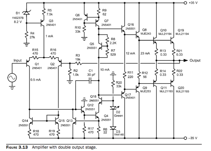
Attached below is my schematic.
Now, these are the problems I'm experiencing:
1. I have 7V of DC offset at any supply voltage from +/-12 to 30V.
2. If I raise the bias current above about 30mA the current draw from the PSU will suddenly raise to about 1A with some oscillation on the output with 7V offset.
3. I do get a good looking output signal however the gain is small and will start oscillating on the negative half above about 2Vpp on the output.
I can tell you the input transistor base (Q2) is at 0V and the base of Q3 is at 1/20 of 7V.
The tail current for the input stage is 1mA (the designed amount) and the legs have approx 500mA in each.
The VAS has the designed 10mA running through it.
I see the large DC offset reflected in the VAS too.
That's about it at the mo. Please if anymore information is needed I'll get it. Any help would be fantastic!
Thank you!
I was looking for a reasonable amplifier to build for a multi channel system. I like Bob Cordell's book and so decided to try and build an amplifier he goes through in there but I'm having some issue with it on the bench. This is the Cordell amplifier:
Attached below is my schematic.
Now, these are the problems I'm experiencing:
1. I have 7V of DC offset at any supply voltage from +/-12 to 30V.
2. If I raise the bias current above about 30mA the current draw from the PSU will suddenly raise to about 1A with some oscillation on the output with 7V offset.
3. I do get a good looking output signal however the gain is small and will start oscillating on the negative half above about 2Vpp on the output.
I can tell you the input transistor base (Q2) is at 0V and the base of Q3 is at 1/20 of 7V.
The tail current for the input stage is 1mA (the designed amount) and the legs have approx 500mA in each.
The VAS has the designed 10mA running through it.
I see the large DC offset reflected in the VAS too.
That's about it at the mo. Please if anymore information is needed I'll get it. Any help would be fantastic!
Thank you!
Attachments
There are some parts missing from the attached schematic.
There must be some resistor at the input. The DC blocking capacitor missing from the feedback network.
This amplifier is simply not useful.
OK now I checked the pdf too. Add the DC blocking capacitor series with the 1kohm feedback resistor. It will solve the DC offset.
C5 was not in the original schematic.
Sajti
Last edited:
I have 7V of DC offset at any supply voltage from +/-12 to 30V.
That circuit is for educational purposes, and lacks certain practical refinements.
See p. 76 of the 2011 edition. Resistor R2 requires a series 100uF NP capacitor
to lower the DC gain to unity. That should lower the offset considerably.
Last edited:
When the bias point makes no sense at all, the reason is often parasitic oscillation, possibly close to the fT of the transistors.
Do you measure DC voltages by directly connecting a digital multimeter to the node under test? If so, does the reading change when you solder a 10 kohm resistor to the node and connect the meter to the other side of it? The capacitance of a DMM can sometimes upset the circuit.
If you use a scope, what kind of probe do you use?
If you have a fast scope (> 100 MHz) you could try connecting the ground lead of the probe to its tip and use the whole thing as a magnetic field probe. Move it around above the amplifier to check for signs of VHF oscillation.
Do base stoppers do any good?
Rayma and Sajti, you are right of course: PNP base current through 100.47 kohm amplified 21 times...
depending on your construction, you will most likely need base stoppers.
0.1R output transistor emitter resistors is very low for homebrew; i'd recommend going larger (at least 0.22R) unless you are VERY confident about the bias arrangement and thermal design.
also, how is the bias transistor monitoring the output transistor temps to the output transistor heat sinks?
so, why don't you share some pictures? it may help get you more specifically helpful comments.
but, good job jumping in and trying to build something!
mlloyd1
Thanks, everyone, for the comments.
I'll be trying out your suggestions this weekend. I do struggle to see how I get 7V of offset at the output just from not having a cap in the feedback path. Could this be caused by mismatch in the input transistors? With 7V/21 that will still give me ~330mV of offset on the output which is still unacceptable. This makes me think the issue is elsewhere like D2 voltage not being high enough.
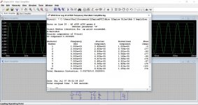
I'm using a 300MHz probe to take my measurements. When the amp draws more current it does start oscillating, this happen randomly or when I try to crank up the bias.
I posted this amp before and people said it's not finished, but other than a cap to remove the DC gain what's missing?
I've ordered some 0.33R resistors for bias.
I asked about it's incompleteness in a different thread but after everyone pointed it out I got very few reasons for it. Could anyone point out what t's missing?
Thanks!
I'll be trying out your suggestions this weekend. I do struggle to see how I get 7V of offset at the output just from not having a cap in the feedback path. Could this be caused by mismatch in the input transistors? With 7V/21 that will still give me ~330mV of offset on the output which is still unacceptable. This makes me think the issue is elsewhere like D2 voltage not being high enough.
I'm using a 300MHz probe to take my measurements. When the amp draws more current it does start oscillating, this happen randomly or when I try to crank up the bias.
I posted this amp before and people said it's not finished, but other than a cap to remove the DC gain what's missing?
I've ordered some 0.33R resistors for bias.
I asked about it's incompleteness in a different thread but after everyone pointed it out I got very few reasons for it. Could anyone point out what t's missing?
Thanks!
how I get 7V of offset at the output just from not having a cap in the feedback path.
Could this be caused by mismatch in the input transistors? other than a cap to
remove the DC gain what's missing?
Designing a stable, direct-coupled power amplifier with 0VDC offset is difficult.
Usually a servo or a unity gain capacitor in the nfb loop is necessary.
Using matched input devices, thermally coupled, does help.
A practical and reliable amplifier will look much different from a textbook circuit.
Each design is unique, and can take much time to bebug. A finalized version
of this circuit did not seem to be in the book. It's very likely that there are
multiple issues that need attention before the textbook circuit will work properly.
Last edited:
Sugestions
Dear Boscoe,
If you allow me to oppinate, I suggest you to add a small elco capacitor across D1 (8v2 zener) and redirect R6 to the junction of D1 and R17. With these changes you will improve PSRR.
I also suggest you to add small capacitors in parallell with Base - Collector junction of Q17 and Q18. It will manage output stage instability. You can start with 100pF but 22pF is enough to most applications.
Those changes I need to do simulating Bob Cordell schematics.
Regards
Ronaldo
A practical and reliable amplifier will look much different from a textbook circuit.
Can you expand on what? And if there's anything I haven't done in my practical example that I should have?
Thanks!
own
See fig. 3.16 for starters. Adding these functions should help at least some of your problems.
I can't find this amp actually built-up and working anywhere, but Maybe Bob can reference
a fully working version of this circuit, either his, or one someone else built.
if there's anything I haven't done in my practical example that I should have?
See fig. 3.16 for starters. Adding these functions should help at least some of your problems.
I can't find this amp actually built-up and working anywhere, but Maybe Bob can reference
a fully working version of this circuit, either his, or one someone else built.
Last edited:
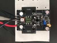
Here's a picture of my PCB.
Looks good, are you using a lab supply with current limiting?
Sometimes those can cause problems too. But, first address the
missing parts shown in in Fig. 3.16, since it can't work without those.
Thanks, everyone, for the comments.
I'll be trying out your suggestions this weekend. I do struggle to see how I get 7V of offset at the output just from not having a cap in the feedback path. Could this be caused by mismatch in the input transistors? With 7V/21 that will still give me ~330mV of offset on the output which is still unacceptable. This makes me think the issue is elsewhere like D2 voltage not being high enough.
I'm using a 300MHz probe to take my measurements. When the amp draws more current it does start oscillating, this happen randomly or when I try to crank up the bias.
I posted this amp before and people said it's not finished, but other than a cap to remove the DC gain what's missing?
I've ordered some 0.33R resistors for bias.
I asked about it's incompleteness in a different thread but after everyone pointed it out I got very few reasons for it. Could anyone point out what t's missing?
Thanks!
The input transistor's base current flows to ground through 100.47 kohm of resistance. The transistors are biased at about 500 uA each and their hFE is between 50 and 240, typically 100 (see http://www.mouser.com/ds/2/149/MMBT5401-889782.pdf). Hence, one would expect a typical voltage drop of about 500 mV, but it be anything between 200 mV and 1 V. Amplify it 21 times and you can easily get 7 V of offset.
A capacitor in series with R14 will reduce the offset roughly 21 times, because the DC gain is reduced from 21 to unity. With the capacitor added, you can reduce R15 to 18 kohm or 20 kohm such that R15 + R19 ~= R13. This will reduce the DC voltage across R15 + R19 and if the input transistor's hFE's match, the drop across R13 due to Q3's base current will then cancel the drop across R15 + R19.
The only thing that doesn't quite add up is your claim that Q2's base is at 0 V. It can't be unless the amplifier is switched off.
The return path of the front end supply bypass caps could perhaps be tied to PGND instead. Not seems to be a good idea to get them return currents to pass R21. By the way I can't seem to be able to locate R21 in the PCB picture. Is it on the opposite side?
The C9 in the schematic has a 50V rating, I hope you used a higher voltage rating part than that in the actual build, that is able to withstand total combined voltage of both rails.
The C9 in the schematic has a 50V rating, I hope you used a higher voltage rating part than that in the actual build, that is able to withstand total combined voltage of both rails.
> I do struggle to see how I get 7V of offset at the output just from not having a cap in the feedback path.
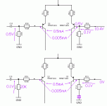
Just figure the actual resistance, current, voltage, gain relations around the loops. Simple networks. No great accuracy needed here. NO SPICE NEEDED! Matchbook and a few fingers. See Attached. I rounded the hFE of a '5401 to "100" and got an error some higher than yours. Smells like your '5401s are hFE~~140, which is OK by the datasheet.
> mismatch in the input transistors?
No; mis-match of base REsistors.
Analysis below assumes perfect match. Mis-match will cause an additional error. But if you make Q2 base resistor "small", resistor drop is small, and mismatch error will be small. If you additionally put the _DC_ gain to unity (the cap), the errors will not be multiplied by the audio gain (makes them 21X bigger).
Attachments
Last edited:
A practical and reliable amplifier will look much different from a textbook circuit.
This design for educational only. If you understand what Bob Cordell said in his book, you will able to implement it in practical amplifier.
Each design is unique, and can take much time to bebug.
Almost all my amplifier is working in first time, no need for debugging. But if you want the amplifier work as your plan (in simulation), you need tweak it.
Looks good, are you using a lab supply with current limiting?
Sometimes those can cause problems too. But, first address the
missing parts shown in in Fig. 3.16, since it can't work without those.
Thanks! But have you looked at my schematic? It has all of those other than the feedback DC blocking cap.
The return path of the front end supply bypass caps could perhaps be tied to PGND instead. Not seems to be a good idea to get them return currents to pass R21. By the way I can't seem to be able to locate R21 in the PCB picture. Is it on the opposite side?
The C9 in the schematic has a 50V rating, I hope you used a higher voltage rating part than that in the actual build, that is able to withstand total combined voltage of both rails.
> I do struggle to see how I get 7V of offset at the output just from not having a cap in the feedback path.
Just figure the actual resistance, current, voltage, gain relations around the loops. Simple networks. No great accuracy needed here. NO SPICE NEEDED! Matchbook and a few fingers. See Attached. I rounded the hFE of a '5401 to "100" and got an error some higher than yours. Smells like your '5401s are hFE~~140, which is OK by the datasheet.
> mismatch in the input transistors?
No; mis-match of base REsistors.
Analysis below assumes perfect match. Mis-match will cause an additional error. But if you make Q2 base resistor "small", resistor drop is small, and mismatch error will be small. If you additionally put the _DC_ gain to unity (the cap), the errors will not be multiplied by the audio gain (makes them 21X bigger).
The input transistor's base current flows to ground through 100.47 kohm of resistance. The transistors are biased at about 500 uA each and their hFE is between 50 and 240, typically 100 (see http://www.mouser.com/ds/2/149/MMBT5401-889782.pdf). Hence, one would expect a typical voltage drop of about 500 mV, but it be anything between 200 mV and 1 V. Amplify it 21 times and you can easily get 7 V of offset.
A capacitor in series with R14 will reduce the offset roughly 21 times, because the DC gain is reduced from 21 to unity. With the capacitor added, you can reduce R15 to 18 kohm or 20 kohm such that R15 + R19 ~= R13. This will reduce the DC voltage across R15 + R19 and if the input transistor's hFE's match, the drop across R13 due to Q3's base current will then cancel the drop across R15 + R19.
The only thing that doesn't quite add up is your claim that Q2's base is at 0 V. It can't be unless the amplifier is switched off.
Thank you, all, for your feedback. I will be trying this tonight! Will let you know how I get on.
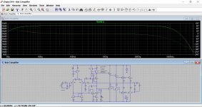
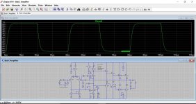
I had a play with this and have attached the .asc if anyone wishes to continue. I made a few quick changes but found the stability might need looking at more closely. The last shot shows something going on but whether it is an artefact of the sim I wouldn't like to say. However other tweaks I tried also showed stability issues (such as decoupling the vbe multiplier).
Attachments

- Status
- Not open for further replies.
- Home
- Amplifiers
- Solid State
- Please help with issues I'm having with my Bob Cordell amplifier implementation.