When I’m making a PCB that is simple and has large components, I prefer using good old pencil CAD to design my PCB layout.
After I've drawn the layout, I drill the holes for all my components. Then I cut my traces by hand with a rotary tool.
To eliminate dust from flying all over, I cut the traces with the PCB submerged in about ½” of water. No need for etching chemicals.
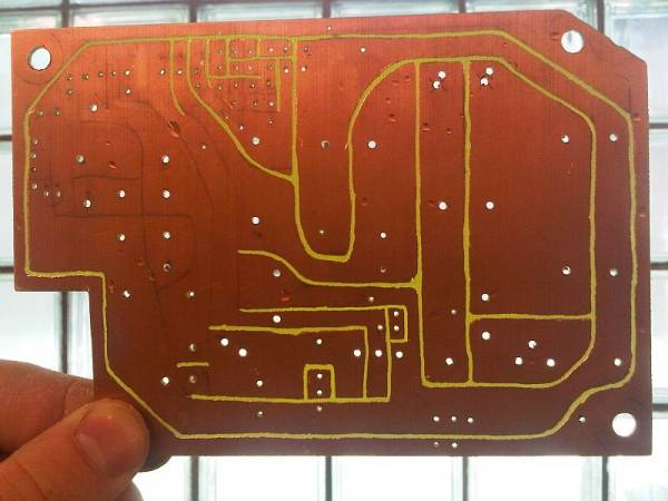
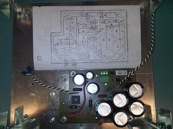
Here you can see the pencil layout and finished PCB.
After I've drawn the layout, I drill the holes for all my components. Then I cut my traces by hand with a rotary tool.
To eliminate dust from flying all over, I cut the traces with the PCB submerged in about ½” of water. No need for etching chemicals.
Here you can see the pencil layout and finished PCB.
I remember when I first started out in electronics, making PCBs seemed like an impossible task since you needed all the chemicals, CAD programs and equipment.
When I got out into industry I found it wasn't uncommon to just carve the traces on PCBs. Sometimes you just need like one extra little relay PCB in your project, so this is a quick and dirty way to get it done.
So if you are an electronics hobbyist who hasn’t seen this done before I hope this post gives you another option for board making.
It is a good way of doing basic prototypes, a similar technique was used in the late 80's and is still used today, though layer numbers means its pnly used for simpler designs.
Prototype PCB Milling and Drilling - LPKF Laser & Electronics AG
Prototype PCB Milling and Drilling - LPKF Laser & Electronics AG
- Status
- Not open for further replies.