I recently made a board for a 49600 device. It is the only SMD device in the circuit. I used a primitive stencil kit (still useful ) that I cut down and I found it to be a little difficult for this application. My eyesight is terrible and I have the hands of a diesel mechanic.
I looked around for stencils for more modern devices. High on my list would be stencils for DIP-8, power SMD packages, and popular chip amps like the 3886 etc.
All I found was a "PCB in a Box" kit for $75. This is a new technology for me (I was aware of it) and I don't know how helpful it would be. Can I download stencils from manufacturers to use on my PCBs? That would probably be enough incentive for me to give it a go.
I've been making PCBs since the 70s (I'm not claiming to be very good at it) and my motivation is that I want to use some of the new generation of devices that are not offered in through hole packages. So any advice is much appreciated.
I'm not sure what you mean by "PCB Stencil". The PCB stencil I'm familiar with is used for automated soldering of SMT printed wiring boards (PWB). It's a sheet of very thin stainless steel with cutouts over the places where copper soldering pads appear on the PWB. In production it's aligned with a bare PWB, then solder paste is spread over the stencil. The solder paste goes through the stencil openings and covers the copper pads. Then the stencil is pulled back, the SMT components are placed on their appropriate pads, and the whole assembly is heated to melt the solder, attaching and connecting the components in the process.
Component manufacturers typically publish suggested "padstacks" for their components, showing the size and relative locations of the copper pads as well as the openings in the solder stencil, the location of the solder mask, and even the silk-screen component outline. Typically this is shown as a dimensioned drawing although some manufacturers provide the information in the form of library files in the format(s) of popular PWB layout software.
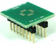
Are you thinking of SMT adapter boards, to which you solder an SMT component and the board "enlarges" the connections to mate with DIP or other through-hole patterns? There are several suppliers - seed a search engine with "smt adapter".
Dale
Component manufacturers typically publish suggested "padstacks" for their components, showing the size and relative locations of the copper pads as well as the openings in the solder stencil, the location of the solder mask, and even the silk-screen component outline. Typically this is shown as a dimensioned drawing although some manufacturers provide the information in the form of library files in the format(s) of popular PWB layout software.
Are you thinking of SMT adapter boards, to which you solder an SMT component and the board "enlarges" the connections to mate with DIP or other through-hole patterns? There are several suppliers - seed a search engine with "smt adapter".
Dale
Attachments
You must work in industry. I've made PCBs with enamel that you paint on, and stencils that you press on. I know that there's a way to CAD design them at home and "print" a stencil with a home printer and I was hoping for some comment on this, and other "do at home" procedures.
I've seen those and they were in the back of my mind. I will look into that. Thanks, Dale.
I still want to make some better boards at home.
Are you thinking of SMT adapter boards, to which you solder an SMT component and the board "enlarges" the connections to mate with DIP or other through-hole patterns? There are several suppliers - seed a search engine with "smt adapter".
Dale
I've seen those and they were in the back of my mind. I will look into that. Thanks, Dale.
I still want to make some better boards at home.
This looks like it could be adapted for some chip amps. Invalid Request And this too. Invalid Request
This looks useful. http://www.digikey.com/product-detail/en/DE-54/DE-54-ND/6983 This too. http://www.digikey.com/product-detail/en/416-ER/473-1104-ND/2425855
And here's what I used to make boards way back in the day. http://www.digikey.com/product-detail/en/22-0220/GC220-ND/108553
A search for "etching and fabrication equipment" produced these results.
Last edited:
I haven't seen any of those since the 80's !!!
I use a plain ole' Sharpie pens for an etch resist pen when I need it.
I have made a few boards using just them as well, But my drawing ability is not at all good, but it works!!! He,he,he
Here is a link to a video I found a while back on how to make your own stencils out of aluminium pop cans,
http://www.diyaudio.com/forums/construction-tips/221683-smd-soldering.html#post3706421
FWIW
jer 🙂
I haven't seen any of those since the 80's !!!
You mean the press on stickers? They still work. 🙂 And now I've found some kits that are much handier for what I'm doing.
I just heard about the Sharpie, but I haven't used it. I heard that if you shake the Sharpie like a thermometer, the tip gets very wet and works great for etch resist. Those pens I linked to are probably just glorified Sharpies.I use a plain ole' Sharpie pens for an etch resist pen when I need it.
I have made a few boards using just them as well, But my drawing ability is not at all good, but it works!!! He,he,he
The first etch resist tool I ever used (back around 1974 or so) was a bottle of black goop with a little application brush attached to the cap. It worked. 😀
That is so very cool. I haven't used solder paste. In fact the only reason I'm messing with SMD is because so many of the new generation of devices are available in SM packages only. Right now I am only interested in integrating SM devices with through hole boards.Here is a link to a video I found a while back on how to make your own stencils out of aluminium pop cans,
[URL="http://www.diyaudio.com/forums/construction-tips/construction-tips/const...ml#post3706421"]http://www.diyaudio.com/forums/const...ml#post3706421[/URL]
I just tin the board with silver solder, then tin the device leads, then I clip the device to the board and heat the pins with the iron. Then I mop up with solder wick. This is how a caveman would do it, and it works.
Last edited:
The Stickers as you call them were rub on transfers, I had a friend that used to use them a lot.
I found them a bit tedious to use, I much prefer using the laser toner transfer method.
I get great results from that method, Here I show my very First go at it for a SMD part,
http://www.diyaudio.com/forums/construction-tips/221683-smd-soldering.html#post3685868
I manually soldered that part as well, Just use a lot of no clean paste flux and the solder won't bead up (too much) and you can just use gravity to pull the excess away from the part.
I too have been forced to learn the ways of SMD, But it is much easier than it appears to be for the most part.
I have been in the process of making patterns of adapter boards for use in the TH board places using dip trace.
Then I just print off a whole sheet of one type of pattern, then I can just cut out a section to iron on as I need to the copper clad material.
I wanted to make a bunch of patterns and post the files, but they are rather large file sizes as I use a 1200 DPI setting for making them.
jer 🙂
I watched that video and was impressed by what he was able to do. Gives me another reason to try toner-transfer sometime. My intuition suggests that the video's producer may have glossed over the practical difficulties of two points: getting the cylindrical aluminum can stock flattened, and avoiding over-etching the stencil openings. (Aluminum doesn't hold up well against acid, and I suspect the time window for getting the aluminum out of the acid and under the rinse water is only a couple seconds between "acceptable etch" and "over-etch".) But I haven't tried the process, so that's just an opinion . . .. . . Here is a link to a video I found a while back on how to make your own stencils out of aluminium pop cans,
http://www.diyaudio.com/forums/construction-tips/221683-smd-soldering.html#post3706421
. . .
After watching the video, I thought "Hey - stencils produced with this technique aren't limited to placing only solder paste. 'Fast Eddie' could create a stencil for stenciling an accurate pattern of etch-resistant material - Sharpie ink, nail lacquer, etc - onto a PWB, then manually drawing the pad-to-pad connections.".
But then I realized that if he has the ability to create the stencil with toner-transfer, he can just as easily do a whole PWB with toner transfer. Even so, I can see that it might be useful to have a set of such stencils so you could quickly lay down etch resist for common SMT packages when you want to do a quick experiment with just a few components, and not take the time to do a full PWB.
Dale
After watching the video, I thought "Hey - stencils produced with this technique aren't limited to placing only solder paste. 'Fast Eddie' could create a stencil for stenciling an accurate pattern of etch-resistant material - Sharpie ink, nail lacquer, etc - onto a PWB, then manually drawing the pad-to-pad connections.".
That's exactly what I was thinking.😀
Nail lacquer? I wondered if that would work.
But then I realized that if he has the ability to create the stencil with toner-transfer, he can just as easily do a whole PWB with toner transfer. Even so, I can see that it might be useful to have a set of such stencils so you could quickly lay down etch resist for common SMT packages when you want to do a quick experiment with just a few components, and not take the time to do a full PWB.
Dale
I'm not up to speed on the whole toner-transfer thing. And all I want to do is make some boards for prototyping and building a few circuits.
This whole SMD revolution has forced me out of my comfort zone.😀😀
The toner method is the simplest thing ever but it might take a few tries to get your process down pat, and, what type of paper works best with your printer.
For my Samsung printer I have found that HP photo paper seems to work the best after all of the types I have tried.
I am going to give glossy magazine paper a try next as I have read that is works good too since i have a lifetime stockpile of those. 😉
You need a hot iron I had to try a few of them, I found one with a mechanical thermostat that works the best as the electronic ones seem to limit the high heat range a bit.
Although I do have one that does work well, the others I have tried don't.
I found my B&D mechanical one for $3 at the Goodwiil store!!! 🙂
I too am wondering as to how he got the Popcan aluminium so flat !!!!
I have been thinking about this a lot as I need to figure out a how to make some aluminium window screen flat for use in my desktop ESL's (stators), they always have a curve to them as the material is rolled up when you get it.
I would like to try this method to make some Stator's for some ES phones as well.
I was thinking about annealing and baking them in an oven between to flat surfaces but I am not sure if 550 to 575 degrees would be hot enough?!!!
Any paint that can be removed after it has cured can be used, But just like using a marker you must not get the etchant to hot or else the resist may start to disolve or lift off of the PCB clad.
I have seen other videos of how to do micro etching and it has been said that the weaker solutions of etchant give the best results.
I have seen several different recipes ranging from Salt types and Muratic acid to using Sodium Hypocloride (Lye) or a mixture thereof.
jer 🙂
Last edited:
- Status
- Not open for further replies.
- Home
- Design & Build
- Construction Tips
- PCB Stencils for Popular Devices?