Hi everyone,
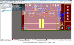
I'm in the final stages of designing a PCB based on the LME49830 datasheet circuit (but using 4 MOSFETs and current sharing resistors) and have run into a question I can't quite answer: I have included a ground loop breaking resistor in my design as well as the footprint for an optional input capacitor. I made the cap optional by including two input terminals, one before and one after the cap. The size of the footprint (dimensioned for 15uF/63V K73-16 caps) means there is quite a long distance between the two terminals and that's where my question came up: I'm unsure whether it would be smarter to route the input ground connection from "before" the cap as closely as possible to the signal all the way up to the LME chip in order to keep the loop area as small as possible (this path would include distance covered by the cap, which is why it "feels" a bit awkward to me) or if I should just use a second loop breaking resistor (or leave those out altogether?) very close to the input terminal and connect it to the ground plane immediately. I hope that makes sense - I'm including 2 pictures to illustrate what I mean. X2 is the input terminal that includes the coupling cap and X1 is the one which bypasses it. The ground line in question is highlighted with white outlines.
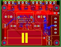
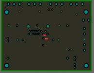
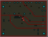
And if someone has general critique/advice regarding my PCB design, I would thankfully accept it as well! The first two pictures are regarding the ground connection issue, the other 3 are the full PCB, ground/power planes and top/bottom signal layers, respectively.
Thanks a lot,
Georg
P.S. I'd be happy to share the design once it's done. I'm using Altium, so if anyone wants to edit it they'll need that, but I'll upload the Gerbers as well.
I'm in the final stages of designing a PCB based on the LME49830 datasheet circuit (but using 4 MOSFETs and current sharing resistors) and have run into a question I can't quite answer: I have included a ground loop breaking resistor in my design as well as the footprint for an optional input capacitor. I made the cap optional by including two input terminals, one before and one after the cap. The size of the footprint (dimensioned for 15uF/63V K73-16 caps) means there is quite a long distance between the two terminals and that's where my question came up: I'm unsure whether it would be smarter to route the input ground connection from "before" the cap as closely as possible to the signal all the way up to the LME chip in order to keep the loop area as small as possible (this path would include distance covered by the cap, which is why it "feels" a bit awkward to me) or if I should just use a second loop breaking resistor (or leave those out altogether?) very close to the input terminal and connect it to the ground plane immediately. I hope that makes sense - I'm including 2 pictures to illustrate what I mean. X2 is the input terminal that includes the coupling cap and X1 is the one which bypasses it. The ground line in question is highlighted with white outlines.
And if someone has general critique/advice regarding my PCB design, I would thankfully accept it as well! The first two pictures are regarding the ground connection issue, the other 3 are the full PCB, ground/power planes and top/bottom signal layers, respectively.
Thanks a lot,
Georg
P.S. I'd be happy to share the design once it's done. I'm using Altium, so if anyone wants to edit it they'll need that, but I'll upload the Gerbers as well.
Attachments


Last edited:
I'm unsure whether it would be smarter to route the input ground connection from "before" the cap as closely as possible
to the signal all the way up to the LME chip in order to keep the loop area as small as possible (this path would include distance covered by the cap,
How about having both inputs near the LME input and the input cap lead, and folding the cap output trace back under the cap?
Last edited:
How about having both inputs near the LME and the input cap lead, and folding the output lead back under the cap?
Thanks for your reply!
I believe that arrangement wouldn't achieve much since the cap lead is also just a wire and having it go back under the cap for several cm would probably lead to a larger loop area than just routing the trace beneath it - I might be wrong though.
I believe that arrangement wouldn't achieve much since the cap lead is also just a wire and having it go back
under the cap for several cm would probably lead to a larger loop area than just routing the trace beneath it
It would minimize the direct input path, though at some expense to the cap path. You can't optimize both in this case at the same time,
unless you use a different cap with leads much closer together.
Last edited:
It would minimize the direct input path.
I'm not entirely sure about that. The path for the DC coupled input would stay the same (assuming I wouldn't move that terminal), and while the ground path for the AC coupled input would become shorter, this would happen at the expense of the signal/hot path as well as potentially moving the ground path farther away physically from the signal path which exposes more loop area to inductive interference, no? Or am I missing something?
Last edited:
I'm not entirely sure about that. The path for the DC coupled input would stay the same
(assuming I wouldn't move that terminal).Of course, you would also move the input connectors to near the LME input, like mentioned in post #2.
BTW, it appears that one lead of C12 is not connected.
Last edited:
I see - moving the second connector closer to the chip would be possible (although it would ruin the last bit of symmetry left in the layout), but I'm still not sure which way to go with regards to the routing of the AC coupled input's ground.I'm not entirely sure about that. The path for the DC coupled input would stay the same
(assuming I wouldn't move that terminal).
Of course, you would also move the input connectors to near the LME input, like mentioned in post #2.
BTW, it appears that one lead of C12 is not connected.
Also, C12 is connected fine - the left lead goes to the ground plane and the right one to the -VEE part of the supply plane. It's a bit difficult to make out from only the pictures. Using 4-Layer PCBs really makes power routing a walk in the park with comparatively simple circuits like this one.
Last edited:
- Status
- Not open for further replies.
- Home
- Design & Build
- Construction Tips
- PCB Routing Advice Needed: How to Handle Input/GND