Good day friends!
-----------------------------------------
UPDATE 2021-09-09
Version 0.6
 Hey! If you are here just looking for the most recent version's:
- Schematic
- BOM
- Gerber files
please head on to Posts:
- #105 : Schematic and BOM
- #108 : Gerber files
If you are interested in the rich discussion prior to those results, keep on reading! 😱
-----------------------------------------
I recently bought the wrong switch! 🙂 A momentary switch instead of a locking one. That triggered an entire process which ended up with the PCB layout I offer here, initially for review / critique from the community, as this is my first PCB design, ever.
So, before getting into details, I would kindly ask that you share any and all comments you can give: ideas, concerns, pointers as to where to research further, anything you consider would be useful. This is not a finished product. Please, do not reproduce (yet!). Eventually, these will be made into publicly available Gerbers.
With that out of the way, here's the On/Off switch PCB literature and motivation, schematics, PCBs and hopefully a lively discussion before this becomes a finished product:
Background
I require a mains switch that works with momentary switches (much more handily available) and that does not see mains current. There is such a project here on this forum, it is Mark Johnson's H9KPXG (PCB: low voltage On-Off switch drives AC mains relay \ includes soft start .. H9KPXG).
Mark's solution has also a soft start, which I don't necessarily need. Also, Mark's solution has an already designed PCB, this project seemed simple enough as for me to give it a shot in designing a PCB with a more or less simple circuit.
Which circuit? Not mine, no... I know nearly nothing about design. Mark kindly pointed me to Rod Elliott's Project 166 (Project 166).
After getting permission from both R. Elliott and M. Johnson to design PCBs based on their solutions, here's what I have come up with:
Those are the basic "highlights" of the design.
Getting into more specifics, here are the schematics and PCBs:
Mains Board + PSU


The mains board is a merging of Project 166's Figure 3 (Typical Mains Switching Circuit) with M. Johnson's implementation of the small brick-type PCB PSUs that I think could be much simpler than using a dedicated transformer and PSU just to drive the relay.
Regarding changes made to P166 design, I have "stolen" (with Mark's permission) his PSU implementation. The biggest highlights are:
What do you guys think? Does it work?
Logic Board


The logic board is a direct implementation of P166 Figure 1 (Push-on, Push-off Switching Circuit).
That's about it. I am unsure about the trace sizes that are recommended for different applications. I have tried to keep:
Again, any feedback of placement, trace size or distribution, building considerations, etc. is very welcome.
Thanks for having a look, best regards,
Rafa.
-----------------------------------------
UPDATE 2021-09-09
Version 0.6
Hey! If you are here just looking for the most recent version's:- Schematic
- BOM
- Gerber files
please head on to Posts:
- #105 : Schematic and BOM
- #108 : Gerber files
If you are interested in the rich discussion prior to those results, keep on reading! 😱
-----------------------------------------
I recently bought the wrong switch! 🙂 A momentary switch instead of a locking one. That triggered an entire process which ended up with the PCB layout I offer here, initially for review / critique from the community, as this is my first PCB design, ever.
So, before getting into details, I would kindly ask that you share any and all comments you can give: ideas, concerns, pointers as to where to research further, anything you consider would be useful. This is not a finished product. Please, do not reproduce (yet!). Eventually, these will be made into publicly available Gerbers.
With that out of the way, here's the On/Off switch PCB literature and motivation, schematics, PCBs and hopefully a lively discussion before this becomes a finished product:
Background
I require a mains switch that works with momentary switches (much more handily available) and that does not see mains current. There is such a project here on this forum, it is Mark Johnson's H9KPXG (PCB: low voltage On-Off switch drives AC mains relay \ includes soft start .. H9KPXG).
Mark's solution has also a soft start, which I don't necessarily need. Also, Mark's solution has an already designed PCB, this project seemed simple enough as for me to give it a shot in designing a PCB with a more or less simple circuit.
Which circuit? Not mine, no... I know nearly nothing about design. Mark kindly pointed me to Rod Elliott's Project 166 (Project 166).
After getting permission from both R. Elliott and M. Johnson to design PCBs based on their solutions, here's what I have come up with:
- A dual board PCB configuration
- One board handles the mains, the relay switch, and a 12v PSU for general use in your system (more on this later!)
- The other boards holds the logic to drive the relay. The idea is that, if anyone favor's something different to the 555 chip, you can simply implement that... hopefully.
- In theory, both boards are stackable as to use less footprint
- Boards adhere to the 10mm mounting hole system widely used in the store, but NOT to the heatsink mounting system. They could be adapted if someone thinks they are useful mounted in the heatsinks, but not likely
Those are the basic "highlights" of the design.
Getting into more specifics, here are the schematics and PCBs:
Mains Board + PSU
The mains board is a merging of Project 166's Figure 3 (Typical Mains Switching Circuit) with M. Johnson's implementation of the small brick-type PCB PSUs that I think could be much simpler than using a dedicated transformer and PSU just to drive the relay.
- First and foremost, credits and attributions: the circuit designer is Rod Elliot, the PSU filtering system is designed by M Johnson. I have included both names on the PCB out of respect, but it is not their "exact" design, so this also may attach their names to something they don't want to. What is the usual practice here? Leave out anything and credit them here? Put something like: "based on", even if its 99% theirs? Please advice as to how is this usually carried out. Thanks!
- It's a dual-layer PCB, but bottom layer only has Ground. Should I just remove the bottom layer, or keep the ground (which mirrors the top layer ground exactly)?
- Instead of laying out 110V or 240V specific layouts, I provided two L+ connectors and two N connectors so that you can pair your transformer secondaries on individual block connectors.
Regarding changes made to P166 design, I have "stolen" (with Mark's permission) his PSU implementation. The biggest highlights are:
- Mark is using a 5V PSU, mine is 12V, so the values of the resistors, capacitors and inductors may not be ideal for this design, I'd appreciate input on this
- I am looking at RTD14012F for the Relay. Maybe 16A is overkill for PREs and other low current uses, and if you want 16A, you probably want Mark's soft start, so maybe a different Relay?
- I talked a bit to an engineer and he believes that C10, C11 and C12 may be 3 different caps to prevent oscillations in three different places of the PCB, and that they may not all be needed. So I kept just one (C3) on the PCB. I'd like also feedback on this, my research may be wrong here and I really need the three caps to filter out the specified frequencies.
- I have left a provision for R3 + C4 to control the current into the coil, but the PCB is laid out in such a way that a single jumper over R3 will remove the entire block if you want to keep the original P166 design without any changes
- I have left a provision for Mark's filtering of the PSU, but if you jumper L1 and don't install C1, C2, C3 you get the unfiltered PSU +12V with a single jumper.
- You could avoid the entire earth/chassis protection by not installing R2 and B1 (obviously, then the chassis connector on the euroblock is useless)
What do you guys think? Does it work?
Logic Board
The logic board is a direct implementation of P166 Figure 1 (Push-on, Push-off Switching Circuit).
- It's a dual-layer PCB, with the bottom layer used only for the +12V rail.
- It stacks on top of the other PCB, blocking out the top screws of the bottom euroblock, so that may need some rethinking. At the very least, you want to screw the bottom cables before stacking them. Yes, maybe this is not the best design.
That's about it. I am unsure about the trace sizes that are recommended for different applications. I have tried to keep:
- +12V rails traces have 0.8mm
- Mains traces (110V, N and Chassis) traces have 3mm (and no ground plane near them
- All other traces have 0.4mm
Again, any feedback of placement, trace size or distribution, building considerations, etc. is very welcome.
Thanks for having a look, best regards,
Rafa.
Last edited:
Thanks Rayma... I am wondering if that isn't already R1 + C1 on the "daughter" logic board? Should that be moved to the "Mains" board? Do you think I need that "on top" of the daughter board implementation?
Thanks again,
Rafa.
EDIT: So, just to expand,
CTRL-1 <-> TERM-1
CTRL-2 <-> TERM-2
CTRL-3 <-> TERM-3
Thanks again,
Rafa.
EDIT: So, just to expand,
CTRL-1 <-> TERM-1
CTRL-2 <-> TERM-2
CTRL-3 <-> TERM-3
There is a load on the other board, but it's best to keep a functional circuit block all on one board,
especially for testing and debugging.
especially for testing and debugging.
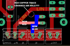
The red-to-red spacing between L and N near the relay, scares me. I recommend moving one trace to the blue layer, allowing far wider spacing between the L and N traces on the red layer. Here's one possibility, done with Paint so there's no 45 degree angles even though 45's are an excellent idea. There are lots of ways to accomplish the "more spacing red to red" goal.
I also think you need to recalculate a proper value of "R3" ... 62 ohms was good for a 5V relay coil, but your relay coil takes 12V not 5V. You want R3 to be something like 33% to 100% of the coil resistance. Smaller resistance is safer (and zero ohms is safest of all!) but bigger resistance extends the life of the relay by dissipating less power in the coil.
_
Attachments
Thanks so much friends for the input! It's really appreciated.
Here are the new schematics and PCB layouts for the Mains board:


Anything else that should be addressed? Any other concerns / suggestions are always highly appreciated.
Thanks,
Rafa.
- Following JPs and Mark's concerns (scares!) about spacing / creepage, I have moved the N traces to the bottom layer as per Mark's drawing, thanks!
- As per Mark's question regarding the trace over air holes 😱 I had no idea those were supposed to be air holes, I was not providing for a perforation on that area. The spec sheet only listed a circle there, no information as to what they are, no picture either. 😱 Thanks for catching that up, I have added vent holes in that area
- As per Mark's suggestion regarding R3, thanks, I had no idea what that R3 was there for and that it had to match Coil resistance. The spec sheet mentions 12V coil resistance of 360 ±10%, so I have changed R3 to 320R (I also believe that the drilling size for R3 was wrong, I have revisited the size on the PCB). It sits just under a full 10% variation (324 Ohms), but if 320 fails to work, I could always replace with 300R.
- As per Rayma's suggestion, I have added provision for R4 10K between CTRL and V--, thanks. As with other modifications to the original P166 schematic, one could simply omit R4 and the circuit would be as the original.
Here are the new schematics and PCB layouts for the Mains board:
Anything else that should be addressed? Any other concerns / suggestions are always highly appreciated.
Thanks,
Rafa.
.....Here are the new schematics and PCB layouts for the Mains board:....
It's late here, maybe I'm missing it--
This started because you had a non-latching switch. So you had a '555 to latch the on/off state.
Then you got suggestions on spacing and holes. Good. But now I don't see any latching mechanism?
PRR, the latching mechanism remains unchanged from the smaller PCB posted on post one. Since there was no comment on it, I did not change anything to it, nor re-posted it in the last post. Nonetheless, it should still be considered part of the entire circuit, and the “OUT” of the “logic board” needs to be connected to the CTRL input of the “Mains Board”.
Maybe I’m missing something or not understanding your concern? Sorry if I’m making things more confusing,
Rafa.
Maybe I’m missing something or not understanding your concern? Sorry if I’m making things more confusing,
Rafa.
Thanks for the info on regulations. Just to be clear, is it jus the “chassis” trace that needs to be increased? Or the L and N as well? I have not seen any trace of 7mm in any PCB I have handled or even seen. Even the H9KPXG seems to have around 3mm for the Chassis trace.
7mm is going to be tough to fit.
Thanks again,
Rafa.
7mm is going to be tough to fit.
Thanks again,
Rafa.
Ordinary thermal starters work like that, you can read up on those, and use that knowledge to improve your circuit.
Single and three phase motor starters, with a thermal relay and contactor - they can be turned on and off using an internal or external momentary contact switch pair, one for each action. I think NO and NC pairs are used, so you can use a change over relay, I think.
That switch sees mains voltage, so you can use something activated by low voltage to trigger the starter action, on or off.
May I suggest to use an onboard PCB fuse directly after the L* connection? It would ensure safety in case the builder "forgets" to add a chassis mount fuse holder (which is BTW more work and more wiring!). Whatever the reasons are, combining the 2 circuits on 1 single board would make things simpler and more reliable. There seems no point in separating the circuits as they won't work without each other?!?! When simple stuff just works not many will replace the 555 part....
Since it is a mains voltage related circuit already adding a mains filter is a simple but very useful thing to do. I think I would even add a separate filter for the switcher (I never use those as transformers don't pollute mains voltage). When you also add a PCB mount IEC inlet with built in fuse stuff can be small and practical. Less wiring, less connections = higher safety/reliability. Just some suggestions...
*normally we use the 3 pin PCB connector but then the version with the middle contact missing for L/N connections. That ensures enough clearance. A PCB mount fused IEC inlet would make stuff absolutely better though.
edit: if you would use a fused IEC inlet with a switch you can disconnect the device from mains when on holidays etc. After having analyzed a few incidents with permanent mains connected stuff going bad I only trust true hard switches.
Last edited:
If we can apply DIN EN 60664-1 Cat. II (the use of IEC inlet must be guaranteed) we can reduce creepage between L/N and châssis to 3mm.
Please use net class option in EAGLE so DRC checks the creepage.
JP
Please use net class option in EAGLE so DRC checks the creepage.
JP
Thanks once more for all the info! and the lively discussion.
So, yes, this will be used with a fused + filtered inlet, I have purchased a Schurter already, this one: 3-105-315 Schurter | Mouser.
So yes, that should be a requirement to switch off the current to the always-on 12V circuit.
I’ll look into the net class option. Thanks.
Will that inlet change the need for the 7mm traces? Thanks again,
Rafa.
The “original” reasoning was more due to inexperience. Having never done a PCB, I thought it simpler to deal with as few components as possible to learn how to untangle the connections and position components.…Whatever the reasons are, combining the 2 circuits on 1 single board would make things simpler and more reliable. There seems no point in separating the circuits as they won't work without each other?!?! When simple stuff just works not many will replace the 555 part....
In the aftermath, I may be pushing the limit on Eagle for free usage, which is 80cm2, but I guess they could be made into a single PCB.
The benefits I saw from this were:
- Mains board can be used with some other logic, or even a latching switch without any board (this could be wrong though, need to check on that)
- As is, if you omit the actual Mains section (relay, BJT and the line outputs), Mains board can also be a small 12V PSU module. Since any PCB manufacturer will force me to buy at least 5 I thought that could be useful
- Use a bit less footprint into the chassis, penalizing vertical size, so you can choose if you want them side by side or on top, depending on your cases.
But, now that I feel more comfortable with the software, I could look into combining all in a single PCB and see how it works, yes, absolutely worth the shot, thanks.
I’ll read into those, thanks. Still, this was an exercise in creating a PCB from a known circuit with as few mods as necessary. I am not even in the same vicinity of being able to create my own circuit or “improve” on it at this point. So changes that come from the actual implementation (like replacing the PSU, or separating the boards) are important, but I think this is not the time to reinvent the circuit as is.Ordinary thermal starters work like that, you can read up on those, and use that knowledge to improve your circuit...
Thanks,
Rafa.
Yes, yes, I’m not trying to justify myself, just convey my train of thought and what led to some choices, I agree some may not be ideal. Still, the reason was to try my hand at something simple where I could learn about PCB placement, trace sizes and spacing, PCB hole sizes and mounting holes. Maybe tackling mains voltage was the wrong decision 🙂 .When PCB mount …..
I agree that a fully functional on-board switchable inlet and fuse would be more useful. That would break the 80cm board limit, almost certainly though, I would need to change to kiCad perhaps? I’ll look into it, thanks.
Rafa.
You are busy with good thinking 🙂 Keep as much stuff as possible on the board and keep connections and wiring to an absolute minimum. I am prejudiced, I know, but with mains stuff one really does better by keeping stuff concentrated and wiring free. It's a pity as I had a nice example here but I threw it in the E waste since I mostly use real mains switches.
Last edited:
- Home
- Amplifiers
- Power Supplies
- PCB: Push on / Push off Mains Switch