Hello
I am building an amp based around the Exicon Lateral MOSFETS and have a question regarding a few things.
1. Since I am set for around 250w using a 42vx42v 400VA transformer, I plan to use multiple devices in parallel, however, I do not know which would be the better way to go about it. Use 4 pairs of single die, or two pairs of double die? As I plan to use matched pairs from profusion, I also plan to omit source resistors. Which is the better way to go when paralleling? 2 or 4?
2. Rather than fusing the power supply, I also plan to fuse each MOSFET individually at the rated supply current. This in my eye is two-fold in that I believe that there will be less resistance caused by the fuses, and also in that I would like to test each device for its actual current sharing under load in real-world conditions.
3. Is there a rule of thumb on bias current using the Exicon? Will it be different because I am omitting source resistors?
4. What are some common capacitance's used across gate-to-source for compensation between the P and N devices? In the datasheet it appears considerably wide between the two.
5. What yalls thoughts on the best thermal insulators for these? I have used silipads before, but wonder what the consensus is? Is thermal tape no good? Run of the mill Amazon bulk stuff any good?
6. 42V secondary runs filtered near 60V, am I all clear using 63V caps in the power supply?
Thank You!
If you are getting matched pairs then the bias current should be fairly well shared between paralleled devices. The goal is 50% sharing.
I do not know about gate to source capacitors. You want series R gate stoppers as min and possible zobel R/C from gate to drain.
suggest to get bob cordell's audio power amp book
5. excicons have the source pins on the flange so it is possible to float the HS. if not get the best ins you can. keratherm are supposed to be good.
6. you have to figure on a high line voltage. i'd go with 80V ecaps
post your sch for use to look at.
I would go with the single die devices as 4 of those 125W devices will run a little cooler than 2 of those 250W devices. I am not talking about heatsink temp. but the heat of the actual device.
4. What are some common capacitance's used across gate-to-source for compensation between the P and N devices? In the datasheet it appears considerably wide between the two.
I could easily be out of my depth here, but using Exicon LMOS you are probably already outside of "common" anything. To get matched +/- drive load capacitance you might have to drive your amp at high freq and measure the OP stage current response and dial it in if you expect to optimize.
I agree with Woody if you expect to get 250W RMS out of this many transistors.
Last edited:
Thank you for the replies..
I should clarify that I am now planning on using 4 pairs of single die per channel. I hadn't mentioned that I was referring per channel.
There is the potential to mount the devices directly to the heatsink, however I usually mount it well to the chassis.
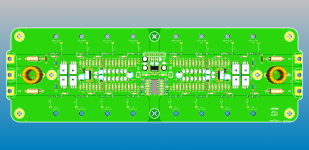
Schematic and board files attached.
While were at it, and since i've nothing yet to test measure, what voltage caps should I be looking to use for both C8 and C14? I like the smallest that I can use.
Bob Cordell's book is apparently $1k paperback on amazon!
Thank You
View attachment 250W.pdf

Last edited:
"Common?" ....... none !!!!!4. What are some common capacitance's used across gate-to-source for compensation between the P and N devices? In the datasheet it appears considerably wide between the two.
Why would you dumb/slow down the better half to make it match the poorer one?
If anything, use driver transistors which can easily drive the higher capacitance ones, and who will find it easier still to drive the better one.
And in any case, asking for "common" values is not the way to design , if anything do your own Math as needed.
Make sure you put a fixed resistor across your bias pot to protect the output stage in case the wiper resistance increases.
I use 100p on the n-FETs and 18p in series with 22R on the p-FETs. Don’t forget zeners and diodes to protect the gates. I also find 100R gate resistance helps a tad.
Why don’t you want any source resistance?
I use 100p on the n-FETs and 18p in series with 22R on the p-FETs. Don’t forget zeners and diodes to protect the gates. I also find 100R gate resistance helps a tad.
Why don’t you want any source resistance?
Last edited:
I was thinking about those individual fuses that you mentioned.
If one goes I believe the second one will blow short after resulting in DC on output?
With DC protection it will shut down when maybe it wasn't necessary in the first place ?
Seems to me that there's better ways to limit current, for example two sloped I/V limiter.
So we're back at Bob Cordell's book again...
Regards.
Figge.
the 4 pair of single die will run cooler.....................
1. Since I am set for around 250w using a 42vx42v 400VA transformer, I plan to use multiple devices in parallel, however, I do not know which would be the better way to go about it. Use 4 pairs of single die, or two pairs of double die? As I plan to use matched pairs from profusion, I also plan to omit source resistors. Which is the better way to go when paralleling? 2 or 4?
The LatFETs are reputed to be extremely robust and thus there is a chance the fuse/s will blow before the good devices get damaged.2. Rather than fusing the power supply, I also plan to fuse each MOSFET individually at the rated supply current. This in my eye is two-fold in that I believe that there will be less resistance caused by the fuses, and also in that I would like to test each device for its actual current sharing under load in real-world conditions.
Borbely tells us that the minimum LatFET output bias should be at least 500mA. This rule also applies to VertFETs. There is no good reason to omit the source resistors in paralleled devices.3. Is there a rule of thumb on bias current using the Exicon? Will it be different because I am omitting source resistors?
Start with equal value gate stopper resistors. When you have evidence that performance is improved by changing these, then make the change permanent.4. What are some common capacitance's used across gate-to-source for compensation between the P and N devices? In the datasheet it appears considerably wide between the two.
run of the mill sil-pads are not as thermally conductive as thin Kapton nor thin mica. But they are easy to fit (once).5. What yalls thoughts on the best thermal insulators for these? I have used silipads before, but wonder what the consensus is? Is thermal tape no good? Run of the mill Amazon bulk stuff any good?
No.6. 42V secondary runs filtered near 60V, am I all clear using 63V caps in the power supply?................
The output voltage is Mains input/Rated primary * Rated secondary * (1+transformer regulation)
when you input the data for worst case maximum voltage you will end up near 70Vdc at the smoothing capacitors.
There is no good reason to omit the source resistors in paralleled devices.
I used to think that, but would now take the view that there is every reason to omit them.
Adding the resistors can be likened to lowering the overall transconductance of the device (something that is in limited supply with lateral FET's when compared to verticals).
From a current sharing perspective the resistors are of very limited use, thanks to the gentle turn on characteristic of the lateral device.
Borbely tells us that the minimum LatFET output bias should be at least 500mA. This rule also applies to VertFETs.
How so? Four pairs at 500mA each, +/-55V is 220W quiescent. That's just a teeny bit excessive, no?
I run my laterals at ~50mA each pair, and they work very well.
Go and read Borbely's papers. You will see he agrees with many in recommending that, or more.
BTW,
when you get around to reading you will see he refers to total output bias current, irrespective of the number of output pairs used.
I see you contributed to a Borbely thread this year.
BTW,
when you get around to reading you will see he refers to total output bias current, irrespective of the number of output pairs used.
I see you contributed to a Borbely thread this year.
Last edited:
Go and read Borbely's papers. You will see he agrees with many in recommending that, or more.
BTW,
when you get around to reading you will see he refers to total output bias current, irrespective of the number of output pairs used.
Even 500mA total is 55W quiescent. Unnecessary waste of power.
Have you read about cross over distortion?Even 500mA total is 55W quiescent. Unnecessary waste of power.
Have you read that the crossover artifacts are at the higher harmonics and sound particularly nasty?
Have you read that mosFETs do not have an optimal bias for minimising crossover distortion?
Have you seen N.Pass recommending increased bias for mosFETs to minimise crossover distortion?
He and others state the higher the mosFET bias the better they perform.
I run my laterals at ~50mA each pair, and they work very well.
Well I run mine at around 60 ma (but I never tell anyone 😉)
Thanks again for the participation
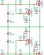
I've updated the components in the OPS schematic, yet, I know in some designs like Rod Elliot, he uses no gate capacitance compensation on the P channel. Is negligible? Omit-able? Perhaps I'll just test and experiment with the gate stopper resistor. Trying to keep it clean. In my PCB design, i've about maximized and minimized each lead and trace, minimizing any possible errors or need for compensations.
For the gate protection, I've used diode and zener diode values based on some other schematics found, are these trivial? I've never used this strategy before.
The fuses on each device are not for protection beyond individual device failure. I've considered leaving those out as well.
Is Cordells book really $1k?
Thanks again

Borbely tells us that the minimum LatFET output bias should be at least 500mA. This rule also applies to VertFETs. .
100mA is usually the bias current spec per mosfet for laterals.
As for vertical mosfets I often get away with as little as 10mA.
I have never had any problems with quality of sound.
"Common?" ....... none !!!!!
Why would you dumb/slow down the better half to make it match the poorer one?
If anything, use driver transistors which can easily drive the higher capacitance ones, and who will find it easier still to drive the better one.
And in any case, asking for "common" values is not the way to design , if anything do your own Math as needed.
If you tune the RC at the N and P gates you can smooth out cross conduction during high slew rate. You can change either R or C or both. Hafler did it. Old DH schematics for example.
If you tune the RC at the N and P gates you can smooth out cross conduction during high slew rate. You can change either R or C or both. Hafler did it. Old DH schematics for example.
Some lateral mosfet pairs need a different gate resistor for N and P channels as gate capacitance is different.
On one lateral datasheet I saw 330r for N and 220r for P specified.
Yes, and with these nifty parts the gate source capacitance and difference beteween N and P types is small, so adjusting for matched response wont exactly ruin overall HF performance.
- Status
- Not open for further replies.
- Home
- Amplifiers
- Solid State
- Paralleling Exicon LMOSFETS