My spec.were:
Device list:
- +/-40-60V input voltage
- +/- 17V 1% output voltage without triming
- 50mA of nominal current
- low noise, low output impedance, low ripple
- simple design
Device list:
RA1
Res.
9,09K
RA2
Res.
9,09K
RA3
Res.
3,65K
RA4
Res.
3,65K
RA5
Res.
5,23K
RA6
Res.
5,23K
RA7
Res.
20K
RA8
Res.
20K
RA9
Res.
9,09K
RA10
Res.
9,09K
CA1
Cap.
10u
CA2
Cap.
10u
CA3
Cap.
10u
CA4
Cap.
10u
CA5
Cap.
33pf
CA6
Cap.
33pf
ICA1
Op. Amp.
LT1677
ICA2
Op. Amp.
LT1677
DA1
Zener
8.2V
DA2
Zener
8.2V
DA3
Sh.Reg.
10V
LM4040
DA4
Sh.Reg.
10V
LM4040
TA1
Bjt
KSC2690
TA2
Bjt
KSA1220
Res.
9,09K
RA2
Res.
9,09K
RA3
Res.
3,65K
RA4
Res.
3,65K
RA5
Res.
5,23K
RA6
Res.
5,23K
RA7
Res.
20K
RA8
Res.
20K
RA9
Res.
9,09K
RA10
Res.
9,09K
CA1
Cap.
10u
CA2
Cap.
10u
CA3
Cap.
10u
CA4
Cap.
10u
CA5
Cap.
33pf
CA6
Cap.
33pf
ICA1
Op. Amp.
LT1677
ICA2
Op. Amp.
LT1677
DA1
Zener
8.2V
DA2
Zener
8.2V
DA3
Sh.Reg.
10V
LM4040
DA4
Sh.Reg.
10V
LM4040
TA1
Bjt
KSC2690
TA2
Bjt
KSA1220
Attachments
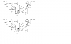
Well it would work but not with those resistor values. The ratio of the voltage divider network at the negative input of the op-amp (RA3/RA5) should be “1+(17(output voltage)/8.2(zener reference) )= 2.073”. Yours is “1+3.65k/5.23k = 1.697” which would give you an output voltage of 13.92V. One other thing is that the current through DA1 which is set by RA1 should be set to the zener test current of the diode which can be found on the diodes data sheet. With RA1 set at 9.09K the current through the zener is slightly less than 1ma which seems too low, this will lower the diode’s reference voltage.
Well excuse me for my device list which is particularly unclear.
On the schematic there is two devices represented as zeners. In fact the voltage réference is not actually a zener it is an LM4040 10V shunt regulator which is suppose (according to its DS) to work very well with less than 1mA.
Regards
On the schematic there is two devices represented as zeners. In fact the voltage réference is not actually a zener it is an LM4040 10V shunt regulator which is suppose (according to its DS) to work very well with less than 1mA.
Regards
Yes but your DA1 and DA2 are the voltage references for you 17V and are listed in your device list as 8.2V zener diodes. Your LM4040's just let the pass transistor turn on enough to get voltage to your op-amp at start up so that it can then regulate to the 8.2V zener that you are using as a voltage reference to the op-amp for your 17V output. So in fact the voltage reference that you are using to compare you 17V to is the 8.2V zener diode and not your LM4040 10V shunt regulator.Or maybe your device list and your schematic don't match?
Last edited:
Yes you are right the device is unclear and there is a mistake in it: the references to to the voltage reference and the zener are inverted.
- Status
- Not open for further replies.