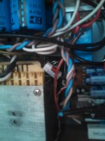
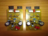
what the function of these diodes? they would be 1N4148? what mistakes on this pcb?
An externally hosted image should be here but it was not working when we last tested it.
Those diodes seem to be between input signal ground and power supply ground. There is a resistor also in parallel. Typically 10 ohms or so. This decouples the two grounds I think . It's covered elsewhere on the forum. I don't use it but you will find it being used by many people.
The resistor between power ground and signal ground is used to lift the small-signal return from the power return, and the diodes in parallel to it limit the extent of the lift to 0.6V for safety reasons.
This assumes that the chassis is connected to mains earth, the power ground is also connected to mains earth, and the RCA connectors on the amplifier are insulated from the chassis.
The resistor alleviates ground loops when externally connected equipment are also connected to mains earth.
The diodes limit the voltage at the RCA barrel to 0.6V away from mains earth, thus protecting the user in case of a mains fault.
I highly doubt the two diodes (1N4148 or similar to my eyes) will help. Those need to carry a lot of current for a short while in fault conditions, and they cannot. It is better to fix any problems upstream, or use a standard loop breaker and keep all the amplifier returns together.
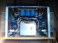
Though I haven't had a look at the PCB in detail, one would be probably better advised to keep both drivers along with Vbe multiplier on one heatsink. This aids thermal tracking and maintains a stable output offset voltage.
This assumes that the chassis is connected to mains earth, the power ground is also connected to mains earth, and the RCA connectors on the amplifier are insulated from the chassis.
The resistor alleviates ground loops when externally connected equipment are also connected to mains earth.
The diodes limit the voltage at the RCA barrel to 0.6V away from mains earth, thus protecting the user in case of a mains fault.
I highly doubt the two diodes (1N4148 or similar to my eyes) will help. Those need to carry a lot of current for a short while in fault conditions, and they cannot. It is better to fix any problems upstream, or use a standard loop breaker and keep all the amplifier returns together.
Though I haven't had a look at the PCB in detail, one would be probably better advised to keep both drivers along with Vbe multiplier on one heatsink. This aids thermal tracking and maintains a stable output offset voltage.

If you read Rod Elliott's article on grounding amplifiers here: Earthing (Grounding) Your Hi-Fi - Tricks and Techniques (see the section "Use of Loop Breaker Circuits") you'll see that the diodes should not be wimpy IN4148 types but power diodes, as they may be called on to handle heavy fault currents without failure - for safety reasons.
As we are talking of fault currents and safety, as an absolute minimum, 10 Amp continuous rated power diodes should be used for even a small amplifier like typical P3a builds tend to be. I don't think that the PCB designer was aware of how the circuit operates and more space will be required in the PBC layout to accommodate the necessary diodes whilst safely conducting the possible fault currents. You would probably need to build and mount the loop breaker assembly elsewhere to fit it and avoid noise pickup problems.
As we are talking of fault currents and safety, as an absolute minimum, 10 Amp continuous rated power diodes should be used for even a small amplifier like typical P3a builds tend to be. I don't think that the PCB designer was aware of how the circuit operates and more space will be required in the PBC layout to accommodate the necessary diodes whilst safely conducting the possible fault currents. You would probably need to build and mount the loop breaker assembly elsewhere to fit it and avoid noise pickup problems.
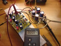
Although I should know better, I use a pair of inverse parallel 1n4002 between the Signal Return and the Power Ground.
And just to confirm , I use a 25A or 35A bridge rectifier double shorted ~ to ~ and + to -
to connect Power Ground to the PE protected Chassis.
And just to confirm , I use a 25A or 35A bridge rectifier double shorted ~ to ~ and + to -
to connect Power Ground to the PE protected Chassis.
Bilbon,
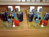
The PCB is one of my earlier attempts in designing my own version of the ever popular P3A, It is my hobbyist perspective not an expert PCB designer. The 10ohm 1N4148 combo serves as a groundlifter as explained by other members here...and yes as Ian Finch stated the assumption is a ground loop breaker is also attached to the system (I'm currently using it, see photo) With regards to the "error", my knowledge is that there are ideal routing of PCB traces laid all over a pcb design. Others are expert on this matter, the lay-out will work just fine however I have made a newer lay-out to which I am currently using over a year now and I do think I successfully extracted the bass character of the amp. I kept on reading that one of P3A highlights is the powerful bass. MY build is an onslaugth of a Category 5 Superstorm pummelling your home 😀
The PCB is one of my earlier attempts in designing my own version of the ever popular P3A, It is my hobbyist perspective not an expert PCB designer. The 10ohm 1N4148 combo serves as a groundlifter as explained by other members here...and yes as Ian Finch stated the assumption is a ground loop breaker is also attached to the system (I'm currently using it, see photo) With regards to the "error", my knowledge is that there are ideal routing of PCB traces laid all over a pcb design. Others are expert on this matter, the lay-out will work just fine however I have made a newer lay-out to which I am currently using over a year now and I do think I successfully extracted the bass character of the amp. I kept on reading that one of P3A highlights is the powerful bass. MY build is an onslaugth of a Category 5 Superstorm pummelling your home 😀
Attachments
abetir, thank you for your explanation. I made two stereo PCB's with your desgin. I'm building a tri-amplified power, one stereo Apex AX-11 for the low frequencies (41+41 Vcc unregulated), one stereo P3A for the mid (30+30 Vcc regulated) and one stereo P3A for the high (24+24Vcc regulated).


Hi MY FRIEND ABETIR!!
YOUR AMPLIFIER !! STABLE VERY STABLE LIKE ROCK
enjoy!
YOUR AMPLIFIER !! STABLE VERY STABLE LIKE ROCK
enjoy!
Attachments
-
 P280914_13.570002.jpg105.2 KB · Views: 572
 -
 P280914_13.560001.jpg168.5 KB · Views: 471
 -
 P280914_13.520001.jpg93.9 KB · Views: 433
 -
 P280914_13.480001.jpg87.3 KB · Views: 1,480
 -
 P280914_13.410001.jpg101.2 KB · Views: 1,555
 -
 P280914_11.100002.jpg142.5 KB · Views: 1,717
 -
 P280914_11.100001.jpg159.1 KB · Views: 2,085
 -
 P270914_21.510001.jpg170.6 KB · Views: 1,835
 -
 P280914_13.590001.jpg103.6 KB · Views: 544
Last edited:
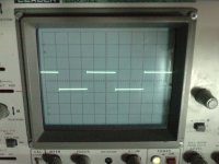
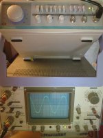
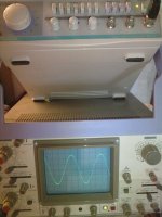
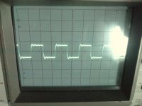
pic 8 shows overshoot and ringing.
What test signal is this? What test load is this?
The pic9 expanded view clearly shows the ringing.
What test signal is this? What test load is this?
The pic9 expanded view clearly shows the ringing.
severe load.
what voltage?
did you try 1nF, 33nF, 100nF, 330nF before you got to 1000nF?
Try with 500mVpp @ output, 1Vpp, 2Vpp, 5Vpp, 10Vpp, 20Vpp?
What if R=16r, 33r, 62r?
what voltage?
did you try 1nF, 33nF, 100nF, 330nF before you got to 1000nF?
Try with 500mVpp @ output, 1Vpp, 2Vpp, 5Vpp, 10Vpp, 20Vpp?
What if R=16r, 33r, 62r?
Solution to the thermal contact between the vbe and drivers in this pcb. It is not the best solution, but I think it should work.
PS: I use google translator, excuse my bad english 😱
An externally hosted image should be here but it was not working when we last tested it.
PS: I use google translator, excuse my bad english 😱
Nikosokey,
Good to hear you back! Another excellent build
Bilbon,
Nice work and this is also how I did it....

Good to hear you back! Another excellent build
Bilbon,
Nice work and this is also how I did it....
Some times i really dont get people .... What is the point of putting so much effort on a pcb that has zobel located above the power transistor ???? While questioning the diodes ?
At some point of stress this can and will cause complications ...There is rules about ground traces and distribution ....
bypass of decoupling is not really usefull where is located , rail location alike
Problem is that the amplifier will produce sound either pcb is loaded with goodies or not
working this way will never achieve numbers though it will play music and satisfy most listeners ....
let me not forget the choice of drivers ....
Sakis,
Thank you for pointing this-out, consider it as "avant-garde" but it also
kept me thinking why not? While most of pcb design had the zobel at somewhere in the midpoint of the PCB, I figure it is impossible to place it near the top of the power transistor because the heatsink gets in the way. But I saw a few that did it differently, zobel goes on top of the power trannies and power trannies goes under with the heatsink (other VSSA is designed this way). One Elektor amp had the zobel almost touching the heatsink. My idea came into fruition while reading some pointers and feedback from other forums who also build the P3A.
Somewhere along the line it seemed to me that a better arrangement
to the CFP output stage is to place the power trannies together with the drivers and zobel network as close as possible. This arrangement is supposedly better in cancelling unwanted oscillation if it ever occurs in a CFP output stage.(My assumption as a hobbyist no hardware measurement done except a DMM and an AnalogMM).I will quote here Bob Cordell's feedback, taken from a forum discussing on zobel
placement.
The first Zobel network, at the raw output of the amplifier, can be important
for high-frequency stability in the output stage, especially when fast transistorsare used. It is desirable that its resistive shunt impedance to ground at high frequencies not be compromized by lead inductance of a wire going off the board if the L-R network is not placed on the board. For this reason, I use a first Zobelnetwork and place it on the PCB near the output transistors. In fact, one can make a distributed first Zobel network of smaller Zobels in parallel and situated among the physical locations of the output transistors.
I also like to use a second Zobel network after the L-R network, and near the speaker terminals. This helps tame speaker cable resonances (or HF standing wave effects) and EMI ingress right at the speaker terminals.
Cheers,
Bob
However as far as I know you are the person with the utmost knowledge and capabilitieswhen it comes to the P3A build. I would also take the opportunity in remindingreaders that all copyright of Project 03 (better known as P3A) belongs to Rod Elliott.The images posted here as of this writing is based on my own PCB design.
Regards!
Yes, I too read R.Cordell's book and these paras fitted in with my understanding of what the amplifier required of the Zobels........................I will quote here Bob Cordell's feedback, taken from a forum discussing on zobel
placement.
The first Zobel network, at the raw output of the amplifier, can be important
for high-frequency stability in the output stage, especially when fast transistorsare used. It is desirable that its resistive shunt impedance to ground at high frequencies not be compromized by lead inductance of a wire going off the board if the L-R network is not placed on the board. For this reason, I use a first Zobelnetwork and place it on the PCB near the output transistors. In fact, one can make a distributed first Zobel network of smaller Zobels in parallel and situated among the physical locations of the output transistors.
I also like to use a second Zobel network after the L-R network, and near the speaker terminals. This helps tame speaker cable resonances (or HF standing wave effects) and EMI ingress right at the speaker terminals.
Cheers,
Bob
......................
And I completely agree with Abe when he arrived at this conclusion. It's exactly the way I understand what the experts tell us. Not just for CFP, it also applies to EF and to quasi outputs.it seemed to me that a better arrangement to the CFP output stage is to place the power trannies together with the drivers and zobel network as close as possible.
Last edited:
Abetir ...Andrew i partially agree with the things you posted even though there is a basis in them juice lays elsewhere
Like all amplifiers the P3A also will be PCB/LAYOUT/STRUCTURE/DISTRIBUTION (signal ground rail output and ground ) depending
I have stated that in electronics is wrong to use patches and cortisone...meaning that amplifier should be solid rock with out them if possible and zobel should be an addition in condition that no load />50% output / HF signal exist one the amplifier .
There is no point to use zobel or patches and medicine to cure oscillation or instability you need to find out where is it coming from and kill it at birth not after.
been producing and testing at least 25 variations of P3A layouts most of them played well but only few of them managed to achieve real numbers given as a fact that there was no variation in the choice of parts ....
Kind regards
Sakis
- Home
- Amplifiers
- Solid State
- P3A PCB