Hello,
I was wondering if anyone had something to say on this small amp and especially on the layout ?
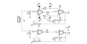
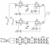
It's a mix of an opa134 at the input and a lm6171 at the output. It's intended to drive higher impedance headphones, like 300 and up. That's why I picked the lm6171 rather than the tpa6120a2 or the ad8397; their high current output isn't really needed.
It will be powered by a +/-9V dc-dc converter followed by a pair of cap multiplier, so it'll probably run at +/-8V.
Inputs at the bottom, outputs at the top of the board.
Thanks for any comment 🙂
PS: it's to go at the output of this thing.
I was wondering if anyone had something to say on this small amp and especially on the layout ?
It's a mix of an opa134 at the input and a lm6171 at the output. It's intended to drive higher impedance headphones, like 300 and up. That's why I picked the lm6171 rather than the tpa6120a2 or the ad8397; their high current output isn't really needed.
It will be powered by a +/-9V dc-dc converter followed by a pair of cap multiplier, so it'll probably run at +/-8V.
Inputs at the bottom, outputs at the top of the board.
Thanks for any comment 🙂
PS: it's to go at the output of this thing.
Attachments
circuit comments:
I wouldn't use the series 220R between the op amps - a Zobel to gnd on that node better terminates/damps the LM6172 input at frequencies above the OPA134 GBW/(loop gain) gain intercept frequency - above that frequency feedback is actually positive and is boosting the OPA's output Z until there's no gain at all
and I'd add output series R, R||L, or lossy bead ferrite bead to isolate the LM6172 from wiring/headphone cable C at 10s of MHz for stability
why pcb? - simple enough to point-to-point for one off stereo amp
if you want to use smt:
why DIP? - heat that doesn't break the chip isn't a problem when the output is inside the loop - noise, offset drift are servoed out by the input op amp gain/global feedback
soic-8 have better high frequency performance than the same chip with the large lead inductance of a DIP
2x soic-8 have better thermal performance than 2 output channels in one DIP-8
and for better analog accuracy physically bigger R at least for global feedback are a good idea to keep their thermal modulation distortion down - low TC NiCr or TaN could help too depending how you land on the practical/tweak spectrum
Last edited:
Hi jcx, thanks for your time 🙂
- wrt the Zobel: I must admit I've never seen one used at this location (most Jung's articles use a 100r resistor there iirc). How would one calculate that zobel ?
- why pcb ? It's for a compact USB DAC (see link ), I might as well put it on the PCB. I'm half decent when it comes to p2p but not good enough to make it fit in such small enclosure.
- why smt: not a lot of room left on the pcb. But I could make r24 to r27 through hole without too much problem, preferably with 1/8W resistors though. Would they be still too small ?
- why DIP: well, it was a kind of trade off in between heat dissipation, space occupied on the pcb and cost (two singles are more expensive than a dual). And dual opamps facilitate the layout too. Maybe am I aiming for too many compromises.
I think your circuit diagram is incorrect with respect to your power decoupling caps, the board looks correct, although the RC network may not be necessary. Also, why not make the 7161 unity gain and eliminate two resistors? You might also need a couple of pF from the 134's output to "-" input, although the 134s tend to be pretty forgiving. Personally, I don't care for tant caps, they're unforgiving with voltages and fail short circuit.
Eagle won't let me have a difference in between schematic and board. But the way the schematic is drawn might be confusing, I'll fix that.
Tantalum caps aren't that bad, really. As a single cap for decoupling, they're packing a lot of capacitance for their size and they're more useful at higher frequencies than common electrolytics. Used, as in here, on a high impedance supply (the 47r serie resistors) and derated (I'll be using 25V caps on 9V), they are actually very reliable. But as soon as there is ripple and low impedance... you're right, best stay away.
As for the gain at the output, it comes from these remarks from jcx: "having gain of 2-4 in the LM6171 local loop helps its stability and adds to the global loop gain avalible for distortion correction in a multiloop" in this thread. As I don't need as much gain as the amp discussed in that thread (overall gain of 10), I kept the gain at 2 for the lm6171 here, to preserve stability with a gain of 4 for the opa134.
Wrt stability. It seems ok as is with the models provided by TI (even with lower impedance loads and some capacitance on the output) but that's only sims... It gets even better with a 100R-10nF zobel at the opa134 output and a 4R7 resistor outside the global loop.
It's true that the opa134 is very forgiving. I've got a "prototype" on single sided pcb with opa134/njm4556 (at unity gain and with a 33pF compensation cap) which doesn't oscillate with a HD650. But I haven't tested it with more difficult loads and my analog scope is limited at 20MHz.
Last edited:
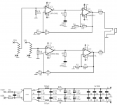
Well, I tried to apply the inputs received. The resistors are now 1206. The resistor in between the opamp is replaced by a zobel. The schematic indicates a lme49713, a lm6171 would work too. A lm6181 also maybe (but with 1k feedback resistors). I switched to single soic packages. A 3R3 to 4R7 resistor is added at the output.
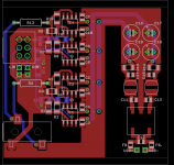
The DC-DC converter is a +/-12V type (Murata MTU2D0512MC). It is filtered for noise but unregulated. It shouldn't be necessary.
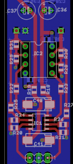
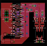
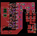
The board is 50*50mm and designed to fit into a 23mm high Hammond enclosure.
The DC-DC converter is a +/-12V type (Murata MTU2D0512MC). It is filtered for noise but unregulated. It shouldn't be necessary.
The board is 50*50mm and designed to fit into a 23mm high Hammond enclosure.
Attachments
Looks pretty good to me
should work just fine as is but of course you can always tweak, but it gets into the judgment/weighting area of whether things can be made better without serious EM Sim or multiple board turns
I do think the Zobel should be terminated to the “high frequency” ground in the middle of the board, I would probably try 100 Ohms, 100 pF
having a “signal gnd” blob on the left is fine, necking down to a join at the headphone TRS gnd is good – if anything I would make it bigger, wider
I am uncertain if the output trace should be rerouted – to minimize loop area they should actually be closer to the power pair
so turning the series thru hole R6,12 (or L?) 180 and giving the out ends pads in the middle power+gnd vertical path and then taping/gluing down jumper wires from their ends to the TRS, bending the wire to conform to the central PS+gnd stripe looks good to me if you don't have 4-layers, aren't worrying about mass production, looks
a circuit change that could be excessive overkill is to sub filter/regulate the OPA134 supplies, referenced/bypassed to the signal gnd blob on the left – can use largish series Z since they don't have much load to drive, and the output op amp local gain means their outputs don't have to swing to the +/-12 rails
another change I would consider is making the fast output op amps LM6172 duals – but paralleled for each channel, independent local feedbacks, outputs summed with few Ohm R outside the local feedback to limit current from offset V without being too big and adding a too low pole with the cable C that could destabilize the global feedback
single LM6171 per channel are fine for 300 Ohm Senns but someone will certainly want to drive heavier loads – if the USB supply can handle it with the ~5x multiplier on current from the DC-DC
but you are the only one who can decide when enough is enough
You may want to try mini- and micro-MELFs for most of the resistors - the thin-film ones have very low excess noise. 0204 mini-MELFs fit easily on a 1206 footprint, and 0102 micro-MELFs on 0603 and 0805 footprints.
Part of the folklore around the LM6172 states that a small rail-to-rail film cap is beneficial to sonics.
For the high-current (inner) opamp, I also looked at the MAX4012/4016, which is spec'ed to drive 50-ohm TL loads. It's limited to +/- 5V rails, but that's fine for a 24-32 ohm load typically used with CMoy-type headamps. It's unity-gain stable, so a pair of them can be used to double the O/P current drive if needed.
Thanks for the comments. I'll go back to the board tonight.
As a general comment, the amp is optimized for my own headphones: senn hd650 (300R) and hd25-13 (600R), akg k340 (360R). None of these require a lot of current but the K340 craves voltage. I just couldn't find a commercial offering (usb-powered) with a 7Vrms output. I might add a grado to the stable at some point but they're fairly easy to drive. If someone wanted more current for lower impedance headphones, he could switch to a +/5v dc-dc converter and replace the output opamp for the max4012 or maybe the ad8397. I wouldn't guarantee stability with that last one though without testing.
linuxguru: thx for the tip on the melf. Never worked with them before, time to start.
jcx:
- thx for the zobel values, I was wondering how to best select them. I'll change the return point.
- changing the left gnd blob: easy enough.
- I'm indeed not worried about looks nor mass production; it should be easy to turn the output resistors 180° around.
- I'll trust you on the excessive overkill wrt to the opa134 PS. 🙂 At first sight, it wouldn't be easy to do it without going to a 4layers board. As it is now, it could be messy mixing feedback and power lines. So I'll pass on this.
- For the dual lm6172, I'd refer to the comment above. For me, coming from OTL tube amps, I'm happy with the lme49713's 100ma.
Allright. I hope it is the last version. 😛 Time to concentrate now on its companion DAC.
The only question I've got left for you is about the position of the zobel under the lme49713 input pins. Is it ok as is ?
The only question I've got left for you is about the position of the zobel under the lme49713 input pins. Is it ok as is ?
Attachments
one thing you likely won't know until you get the part is the DC-DC converter's capacitive coupling noise across the isolation barrier
I used one in a Industrial Instrument design that had middling single digit mA at few hundred kHz
that much common mode current would be an immediate fail of CE EMI when plugged in between 2 gnded components (Desktop PC and disc Player?)
could be an argument for including a 3rd choke in the analog gnd too (I split my isolated supply after the DC-DC, so I was able to use a 2-winding common mode choke)
multiwinding common mode chokes give more Z for their size than multiple uncoupled chokes
Last edited:
Great... a new issue to start reading about.
More seriously: the isolation capacitance of this serie is very low (15pF). So what I'm worrying about is mostly the noise generated by the converter itself more than noise already present on the input, is that right ?
Three lines common mode chokes aren't common (or made for data lines and not robust enough). I can however easily fit a third inductor on the output ground, in between C11/C13 and C14/C15. At the input, a CM choke is easier to find.
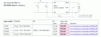
In this app note from Recom, they show different CM filter for the input (p. A-33). Are the caps from input to output truly necessary and should I follow the top or the bottom suggestion (in other words, should I connect a cap from USB-gnd to the 0V output or not) ?
If I push the reservoir caps to the left, I've room enough to add a serious input filter.
More seriously: the isolation capacitance of this serie is very low (15pF). So what I'm worrying about is mostly the noise generated by the converter itself more than noise already present on the input, is that right ?
Three lines common mode chokes aren't common (or made for data lines and not robust enough). I can however easily fit a third inductor on the output ground, in between C11/C13 and C14/C15. At the input, a CM choke is easier to find.
In this app note from Recom, they show different CM filter for the input (p. A-33). Are the caps from input to output truly necessary and should I follow the top or the bottom suggestion (in other words, should I connect a cap from USB-gnd to the 0V output or not) ?
If I push the reservoir caps to the left, I've room enough to add a serious input filter.
I finally found a manufacturer which details class A and B input filters for very similar converters: see here
So I'll use a similar input filter (2.2µF-4.7µH-10µF) and three 100µH inductors at the output in pi config with 2.2µF caps. And 220pF/100V (or more) cap from input gnd to the output gnd.
So I'll use a similar input filter (2.2µF-4.7µH-10µF) and three 100µH inductors at the output in pi config with 2.2µF caps. And 220pF/100V (or more) cap from input gnd to the output gnd.
Attachments
bridging the isolation with a bigger C can cut the common mode noise - laying out for series R+C there gives the option for damping any resonance with the common mode inductance
a downside is the lower Z across the isolation barrier makes a bigger gnd loop at high frequency - trade off time - really needs the hardware, in the full application system to evaluate
a downside is the lower Z across the isolation barrier makes a bigger gnd loop at high frequency - trade off time - really needs the hardware, in the full application system to evaluate

All done and cased (finally 😛 ).
Here's the quick rmaa report. Those figures are for the combined DAC+amp. They're made at 16/44.1, almost 2Vrms into a 100R resistive load. ADC is an ESI Juli@. The figures for the dac alone are here: http://www.diyaudio.com/forums/digi...nnheiser-hd650-request-design-critique-2.html
frequency response (from 40 Hz to 15 kHz), dB / +0.50, +0.45
Noise level, dB (A) / -94.1
Dynamic range, dB (A) / 94.1
THD, % / 0.0018
THD + Noise, dB (A) / -85.7
IMD + Noise, % / 0.0063
Stereo crosstalk, dB / -73.9
IMD at 10 kHz, %/ 0.0072
The whole report (as well as the DAC's) is in the zip attached.
Subjectively, it sounds very clear and shakes up the hd650 beautifully. I'm quite happy with it, but who isn't when a project works out ok ?
Attachments
- Status
- Not open for further replies.
- Home
- Amplifiers
- Headphone Systems
- OPA2134+LM6172 composite amp ?