Frank,
Very strange indeed. Could there be a drawing error in the interconnection of the terminals of those matched pairs? That doesn't make sense.
Jan Didden
Very strange indeed. Could there be a drawing error in the interconnection of the terminals of those matched pairs? That doesn't make sense.
Jan Didden
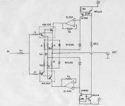
I'm not sure if you read it right, but the dual transistor is in 8-DIP package, so it is represented by the frame outline on a drawing. The power is supplied to one of the collectors, the other collector is connected to the emiter (of the other transistor).
This appears to be a funny and exotic way of cascoding
All transistors appear to work at a fixed Vce of about one diode drop
All transistors appear to work at a fixed Vce of about one diode drop
But that transistor that has the collector to the emitter of the other, that places its collector-base diode in conduction, isn't it? That would influence the operation of the input, no?
Edit: that collector doesn't appear to get any supply, as it is connected (with the other emitter) directly to the output via 10 ohms.
Jan Didden
Edit: that collector doesn't appear to get any supply, as it is connected (with the other emitter) directly to the output via 10 ohms.
Jan Didden
Left side transistors work with Vc = Vb so its Vce is one diode drop
Right side transistors work with Vc = Vb + diode drop so its Vce is two diode drops
Note that left side transistors have its bases tied together while right side transistors have its emitters tied together
Note also that small signal transistors may work with Vce as low as 0.1 V [ie: collector potential between base and emitter potential
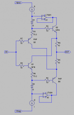
Redrawing the schematic may help to understand it
Right side transistors work with Vc = Vb + diode drop so its Vce is two diode drops
Note that left side transistors have its bases tied together while right side transistors have its emitters tied together
Note also that small signal transistors may work with Vce as low as 0.1 V [ie: collector potential between base and emitter potential
Redrawing the schematic may help to understand it
Thanks Peter, that's MUCH better.
Eva, does that mean that the right side transistor works in what looks like bootstrapped common-base?
BTW, who designed this?
Jan Didden
Eva, does that mean that the right side transistor works in what looks like bootstrapped common-base?
BTW, who designed this?
Jan Didden
janneman said:
BTW, who designed this?
This circuit is used in Mark Levinson ML380 preamp, as well in some other ML units.
Is there a need for dual NPN/PNP transistors here?
Re: Is this better?
Neat!
This is a buffer, right? Looks like a lot of work to replace a piece of wire..😀
Jan Didden
andy_c said:Here's yet another interpretation. [snip]
Neat!
This is a buffer, right? Looks like a lot of work to replace a piece of wire..😀
Jan Didden
Peter Daniel said:
This circuit is used in Mark Levinson ML380 preamp, as well in some other ML units.
Is there a need for dual NPN/PNP transistors here?
I think for best results they should all be matched. Difficult without duals or better, quads. The THAT series quad matched transistor come to mind.
Jan Didden
Re: Re: Is this better?
It's a curved wire without gain
janneman said:Looks like a lot of work to replace a piece of wire..😀
It's a curved wire without gain
It's a diamond buffer with the input collectors bootstrapped to the output
After some redrawing i figured that out but what is the purpose of the opamp+current source?
The current sources force the input transistors to work at a nearly constant Ic
The op-amps work as 'cascodes' and force the output transistors to work at nearly constant Vce
Look how andy_c has redrawn the circuit in a much clear way
The op-amps work as 'cascodes' and force the output transistors to work at nearly constant Vce
Look how andy_c has redrawn the circuit in a much clear way
Thanks Andy_c, only after your drawing it was clear to me what the actual design was.
Funny, how one needs to draw a schematic in a certain way to recognize things. People are severely restricted in this compared to Spice.
Steven
Funny, how one needs to draw a schematic in a certain way to recognize things. People are severely restricted in this compared to Spice.
Steven
The op-amps work as 'cascodes' and force the output transistors to work at nearly constant Vce
Many thanks for the explanation Eva.
Steven said:Thanks Andy_c, only after your drawing it was clear to me what the actual design was.
Funny, how one needs to draw a schematic in a certain way to recognize things. People are severely restricted in this compared to Spice.
Yes, our circuit pattern recognition seems to want to see things in a certain way. I've had circuits I've designed myself put into a CAD system by a draftsman who redrew them in such a way that I could not understand what the circuit was! Curious how the mind works.
If anyone stills looks at this thread, is it by chance the Borbely style? I am slightly lost, but I have been show this,
http://www.diyaudio.com/forums/attachment.php?s=&postid=805978&stamp=1136397897
http://www.diyaudio.com/forums/attachment.php?s=&postid=805978&stamp=1136397897
- Status
- Not open for further replies.
- Home
- Amplifiers
- Solid State
- Ok, I admit i don't make any sense out of this