In the present article offered new way providing thermal stability of the quiescent current in audio amplifiers in the Class AB mode , by changing the current through the measuring and voltage diodes when the temperature of the junctions of the output transistors changes .
Traditionally, to provide the required amount of quiescent current for the output power transistors of audio amplifiers operating in Сlass AB mode, bias circuits are utilized based on diodes, transistors, or a combination thereof, utilizing a decrease of voltage at an open p-n junction with an increase of its temperature when a fixed current flows through it. This dependence is known as about -1,8 mV per degree C. Typically these devices are located on the same heat sink as the output transistors, thereby providing negative thermal feedback, ensuring the necessary quiescent current for the output transistors in AB mode.
On Fig. 1 – Fig. 3 ( pls see attached) are shown classic bias circuits for output transistors operating in Class AB mode. In all of these cases it is necessary to match the quiescent current of the output stage transistors using a potentiometer for each individual amplifier channel, as well as when it is necessary to change transistors.
The ON Semiconductor has released a line of power transistors specifically designed for audio amplifiers that incorporate a diode directly on the transistor chip, called the "Thermal Track" series, which allows, with high precision and design simplicity, ensuring temperature stability of the output stage of an audio amplifier operating in Class AB mode.
Bob Cordell has made some measurements for this devises which indicate that transistor Vbe temperature coefficient is -2,14mV/C while the diode has -1,7mV/C in the case VAS’s current about 9,8mA .Douglas Self showed that for to equalize the temperature coefficients and compensation diodes, it is necessary to reduce the current through the diodes by almost twenty times.
This is possible if the VAS’s current are divided into the two currents: main current and the low-level current, which provides the thermal compensation mode with compensation diodes.
In the present article offered a bias circuit for the output stage of an audio amplifier operating in Class AB mode base on the changing both diode current and his voltage depend from temperature.
If we consider the dependence of the transistor collector current and the forward current through the diode on temperature, it becomes clear that these are two exponentials and are practically identical.
DIODE : TRANSISTOR :
I = Is (e^(V/(nVt)) - 1) Ic= Is * e^(Vbe /Vt)
I — current through the diode Ic — collector current
Is— reverse saturation current Is — reverse saturation current
V — voltage across the diode Vbe — base-emitter voltage
n — ideality factor (typically between 1 and 2) Vt — thermal voltage (Vt= kT/q)
Vt — thermal voltage (Vt= kT/q)
It is obvious that to stabilize the quiescent current of the output transistors, it is more preferable to use both properties of the diode to change both the current and voltage with changes in temperature.
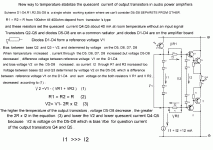
Fig. 4 ( pls see attached) is a circuit diagram displaying principle of operation of the present bias circuit .
The present bias circuit consists of diodes D1, D2, D3, D4, D5, D6, D7, D8 and resistors R1 and R2.
The diodes D1, D2, D3 and D4 are connected in series and inserted into fixed by the current's generator V1 establishing a reference potential for biasing the output stage of the power amplifier, operating in Class AB mode.
To the reference potential, formed by the voltage drop across the diodes D1, D2, D3, D4, through resistors R1 and R2 connected a temperature dependent bias circuit, consisting of the diodes D5, D6, D7, D8, between bases of the transistors Q2 and Q3.
The transistors of the powerful output stage Q2, Q4 and Q3, Q5 are connected according to the Darlington circuit and placed on a common heat sink to dissipate the heat of these output transistors. Resistors R5 and R6 form ordinary circuit of the thermal negative feedback .
Resistors R1 and R2 are elements on which the voltage corresponding to the change in the current flowing through diodes D5-D8 is released when the temperature of the output transistors changes. Thus, the bias voltage of the output transistors on diodes D5-D8 is determined by the difference in the voltage of the reference potential D1-D4 and the voltage drop on resistors R1 and R2. The higher the temperature of the output transistors, the greater the current through D5-D8 and R1 and R2 , accordingly, the voltage on R1 and R2 increases, and the bias voltage of the output transistors decreases.
The diodes D5 and D8 are incorporated directly on the chips of the output transistors Q4 and Q5, respectively. The diodes D6 and D7 are placed onto the same heat sink as the output transistors establishing thermal connection with the heat sink.
In the absence of an amplified signal and at a room temperature of the heat sink of the output transistors, the resistors R1 and R2 of the equal value set the quiescent current of the output transistors Q4 and Q5 through the emitter resistors R5 and R6 to around 40 mA. In the really this resistors set the current through D5-D8 in many times smaller than current through D1-D4 that provided condition matching temperature coefficients Vbe and compensation diodes.
When the signal is amplified, the temperature at the output transistors increases and the quiescent current of the output transistors Q4 and Q5 .The higher the temperature of the output transistors, the greater the current through D5-D8 and R1 and R2 , accordingly, the voltage on R1 and R2 increases, and the bias voltage of the output transistors decreases.
This processes provide temperature stabilization of the quiescent current of the output transistors.
The values of these resistors R1 and R2 are in the range from 100 ohms to 500 ohms depending on the types of output transistors used and are selected for a specific type of transistors based on the value of the quiescent current of the output transistors about 40 mA at a room temperature.
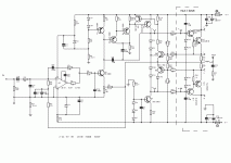
PLS see attached files , there is Explanation of this method and example of the really good working amplifier with same temperature compensation .
Traditionally, to provide the required amount of quiescent current for the output power transistors of audio amplifiers operating in Сlass AB mode, bias circuits are utilized based on diodes, transistors, or a combination thereof, utilizing a decrease of voltage at an open p-n junction with an increase of its temperature when a fixed current flows through it. This dependence is known as about -1,8 mV per degree C. Typically these devices are located on the same heat sink as the output transistors, thereby providing negative thermal feedback, ensuring the necessary quiescent current for the output transistors in AB mode.
On Fig. 1 – Fig. 3 ( pls see attached) are shown classic bias circuits for output transistors operating in Class AB mode. In all of these cases it is necessary to match the quiescent current of the output stage transistors using a potentiometer for each individual amplifier channel, as well as when it is necessary to change transistors.
The ON Semiconductor has released a line of power transistors specifically designed for audio amplifiers that incorporate a diode directly on the transistor chip, called the "Thermal Track" series, which allows, with high precision and design simplicity, ensuring temperature stability of the output stage of an audio amplifier operating in Class AB mode.
Bob Cordell has made some measurements for this devises which indicate that transistor Vbe temperature coefficient is -2,14mV/C while the diode has -1,7mV/C in the case VAS’s current about 9,8mA .Douglas Self showed that for to equalize the temperature coefficients and compensation diodes, it is necessary to reduce the current through the diodes by almost twenty times.
This is possible if the VAS’s current are divided into the two currents: main current and the low-level current, which provides the thermal compensation mode with compensation diodes.
In the present article offered a bias circuit for the output stage of an audio amplifier operating in Class AB mode base on the changing both diode current and his voltage depend from temperature.
If we consider the dependence of the transistor collector current and the forward current through the diode on temperature, it becomes clear that these are two exponentials and are practically identical.
DIODE : TRANSISTOR :
I = Is (e^(V/(nVt)) - 1) Ic= Is * e^(Vbe /Vt)
I — current through the diode Ic — collector current
Is— reverse saturation current Is — reverse saturation current
V — voltage across the diode Vbe — base-emitter voltage
n — ideality factor (typically between 1 and 2) Vt — thermal voltage (Vt= kT/q)
Vt — thermal voltage (Vt= kT/q)
It is obvious that to stabilize the quiescent current of the output transistors, it is more preferable to use both properties of the diode to change both the current and voltage with changes in temperature.
Fig. 4 ( pls see attached) is a circuit diagram displaying principle of operation of the present bias circuit .
The present bias circuit consists of diodes D1, D2, D3, D4, D5, D6, D7, D8 and resistors R1 and R2.
The diodes D1, D2, D3 and D4 are connected in series and inserted into fixed by the current's generator V1 establishing a reference potential for biasing the output stage of the power amplifier, operating in Class AB mode.
To the reference potential, formed by the voltage drop across the diodes D1, D2, D3, D4, through resistors R1 and R2 connected a temperature dependent bias circuit, consisting of the diodes D5, D6, D7, D8, between bases of the transistors Q2 and Q3.
The transistors of the powerful output stage Q2, Q4 and Q3, Q5 are connected according to the Darlington circuit and placed on a common heat sink to dissipate the heat of these output transistors. Resistors R5 and R6 form ordinary circuit of the thermal negative feedback .
Resistors R1 and R2 are elements on which the voltage corresponding to the change in the current flowing through diodes D5-D8 is released when the temperature of the output transistors changes. Thus, the bias voltage of the output transistors on diodes D5-D8 is determined by the difference in the voltage of the reference potential D1-D4 and the voltage drop on resistors R1 and R2. The higher the temperature of the output transistors, the greater the current through D5-D8 and R1 and R2 , accordingly, the voltage on R1 and R2 increases, and the bias voltage of the output transistors decreases.
The diodes D5 and D8 are incorporated directly on the chips of the output transistors Q4 and Q5, respectively. The diodes D6 and D7 are placed onto the same heat sink as the output transistors establishing thermal connection with the heat sink.
In the absence of an amplified signal and at a room temperature of the heat sink of the output transistors, the resistors R1 and R2 of the equal value set the quiescent current of the output transistors Q4 and Q5 through the emitter resistors R5 and R6 to around 40 mA. In the really this resistors set the current through D5-D8 in many times smaller than current through D1-D4 that provided condition matching temperature coefficients Vbe and compensation diodes.
When the signal is amplified, the temperature at the output transistors increases and the quiescent current of the output transistors Q4 and Q5 .The higher the temperature of the output transistors, the greater the current through D5-D8 and R1 and R2 , accordingly, the voltage on R1 and R2 increases, and the bias voltage of the output transistors decreases.
This processes provide temperature stabilization of the quiescent current of the output transistors.
The values of these resistors R1 and R2 are in the range from 100 ohms to 500 ohms depending on the types of output transistors used and are selected for a specific type of transistors based on the value of the quiescent current of the output transistors about 40 mA at a room temperature.
PLS see attached files , there is Explanation of this method and example of the really good working amplifier with same temperature compensation .
Attachments
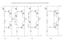


In the second picture of post 1, second and third column, there is a PNP transistor instead of NPN as bias spreader. PNP would be possible, but the other way round.