It's been a while since I have presented an amplifier design here. This one is a "devolution" of another design I have prototyped. The idea is to not use any current sources or current mirrors and to use resistors where possible. "No active loads"
Active loads are allowed in any peripheral circuitry.
The amplifier features symmetrical cascaded LTP driving a symmetrical cascoded cascode VAS with a Thermaltrak output stage.
Compensation is MIC. This MIC also doubles as the lead lag compensation by parasitic shunts via the low impedance feedback network. One of the design goals is to use the minimum number of components (while keeping the basic topology the same) and minimise the number of 0V connections.
Think that the input stage PSRR won't be that good. So the real implementation will have a shunt regulator for the front end.
A few simulated specs:
GNFB loop:
ULGF = 684KHz
PM = 82 degrees
GM = 15 dB
All THDs @ 8R load.
THD1 @ 2.88V = 0.000332%
THD20 @ 2.88V = 0.000960%
THD1 @ 1V from clipping = 0.005387%
THD20 @ 1V from clipping = 0.055248%
Any thoughts, comments, criticisms welcome. 🙂
Paul
PS. I'm still struggling to get the schematics to open at a readable size.... 🙁
Attachments
Last edited:
Congratulations, very interesting design (output EC and all), looking forward to SQ comparisons against some high class amps. 😎
Lazy Cat,
Thank you for the positive feedback. The output stage is a Bob Cordell design. The only thing I changed was using thermaltrak devices for drivers and having low impedance pre-drivers. The local feedback round the output stage is a nice bonus.
Ok, so there was a minor mistake on the previous posting.
So corrected simulated specs are as follows:
GNFB (MIC loop similar)
ULGF = 677KHz
PM = 84 degrees
GM = 16dB
THD1 @ 2.88V = 0.000358%
THD20 @ 2.88V = 0.000996%
THD1 @ 1V from clipping = 0.005769%
THD20 @ 1V from clipping = 0.056176%
Another feature of this design is that the cascodes are not driven from low impedance sources so should not have any oscillation problems.
Also, with the resistor divider for the common base VAS you get an alternative DC servo connection point outside of the signal path.
Paul
Attachments
Update on progress...
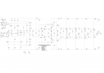
The first change is a slight modification of topology. The cascode VAS has been replaced by a Lender VAS. Gave x5 better distortion performance and saved one resistor. Down side is that the alternative servo connection point has been lost.
Have added some small "speed up" capacitors to the front end. Found cross conduction with large square waves.
The compensation has been re-tuned. The first step was to reduce the LTP degeneration while increasing the compensation caps until the amp slewed in a controlled way from 1V off clipping. Then the feedback network impedance was selected (and compensation caps changed again) to give a "clean" loop gain plot. The last step was to decrease the resistors limiting loop gain to compensate for the decrease in feedback network impedance.
The trade off is: Lower THD, lower slew rate.
The overall design has been tweaked to be low impedance (but still keep dissipations sane).
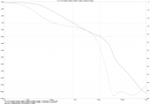
Here's a few simulated specs.
GNFB Loop
ULGF = 789KHz
PM = 87 degrees
GM = 20dB
All into 8R load.
THD1 @ 2.88V = 0.000068%
THD20 @ 2.88V = 0.000220%
THD1 @ 1V from clipping = 0.008614%%
THD20 @ 1V from clipping = 0.009268%
Looks reasonably well behaved overall (so far). 🙂
Edit: Forgot to mention the change to a matched THAT array fro the input BJTs. Also, added the models.
The first change is a slight modification of topology. The cascode VAS has been replaced by a Lender VAS. Gave x5 better distortion performance and saved one resistor. Down side is that the alternative servo connection point has been lost.
Have added some small "speed up" capacitors to the front end. Found cross conduction with large square waves.
The compensation has been re-tuned. The first step was to reduce the LTP degeneration while increasing the compensation caps until the amp slewed in a controlled way from 1V off clipping. Then the feedback network impedance was selected (and compensation caps changed again) to give a "clean" loop gain plot. The last step was to decrease the resistors limiting loop gain to compensate for the decrease in feedback network impedance.
The trade off is: Lower THD, lower slew rate.
The overall design has been tweaked to be low impedance (but still keep dissipations sane).
Here's a few simulated specs.
GNFB Loop
ULGF = 789KHz
PM = 87 degrees
GM = 20dB
All into 8R load.
THD1 @ 2.88V = 0.000068%
THD20 @ 2.88V = 0.000220%
THD1 @ 1V from clipping = 0.008614%%
THD20 @ 1V from clipping = 0.009268%
Looks reasonably well behaved overall (so far). 🙂
Edit: Forgot to mention the change to a matched THAT array fro the input BJTs. Also, added the models.
Attachments
Last edited:
Hi,
Quick question... If one was to put inductors in parallel with the output transistor base resistors what characters would they need to have? For example, what sort of value? Assume they would need to be lossy?
Just laying out the PCB currently and would like to add these as an option?
This is a new idea to me. It may not even be doable and may increase the chances of oscillations.
Any comments welcome.
Many thanks,
Paul
Nice to see the project is ongoing and close to real testing phase. Inductor in parallel to base damping resistor would cause the merged impedance to alter roughly from 0 to 4,7 Ohm in accordance to frequency. More interesting effect would be the phase shift induced to the base current and its correlation with 22 nF base capacitors as these combined forms serial resonance circuit. RL-C would damp base potential at HF meaning tuning resonance to the poles of the output stage is mandatory otherwise the effect could be counterproductive causing oscillation. Value of L would be in a range of uH so the space for little SMD inductor in parallel to base resistor is more than enough on PCB layout. Real testing would show if parallel inductors are necessary or not. Designers quite often use ferrite bead on output transistor's base lead, causing higher impedance/damping at HF.
Looking forward to see no active CCS amp alive and kicking.
Looking forward to see no active CCS amp alive and kicking.
- Status
- Not open for further replies.