Hi all...I do need some help with this schematic. I searched for days and can't find anything similar. Previously, I thought I had problems with the FETs but now both channels are somewhat working (well, sort of, in a limbo mode).
Background: I built this amp 30 years ago when I was in H.K. It is an all MOSFET/FET stereo power amp kit on dual power rails. The manufacturer scrapped off the FET's original part numbers and put something else on it but I can tell the output pair is K60/J19 VFETs. The drivers and the pair on the differential part have no reference of what is the real part number. The schematic is sort of simple (see attached). Most part of the schematic is symmetrical. It didn't work right from day one so it has been in storage for over 30 years. I'm pulling it out, trying to get it working again.
Problem:- Huge DC offset. The working channel has about 200-300mV offset. The not so working side has a 4 to 5 volts DC offset. I measured the FETs with omhmeter and they appear to be ok, though they are not matched between N and P channels. By putting a large DC blocking cap at the output of the bad channel, I confirmed it does amplify sound.
I'm trying to understand the schematic so I can troubleshoot the problem. I read some information that usually the NFB will keep the DC offset low (if the FETs are well match). But if the differential pair is not match, I can get a lot of DC offset.
What I don't understand on the schematic is from TR7,8 towards the power MOSFET, it is symmetrical. But the connection of the gates of TR7,8 to get signals from the long tail pairs are not symmetrical, especially the connection from the gate of TR8 to the two 100ohms (which connect to the sources of the long tail pair). This is the part I can't understand.
I would think the gate of TR8 would get the inverted signal from the drain of TR9 (since TR7 is getting the non-inverted signal from TR10).
What do you guys think with this schematic ? Is TR8 just a dummy (not contributing to amplification) ? Where should I start looking to troubleshoot DC offset ? Should I get some matched pairs of jFETs to replaced those no name components ? Should I put a 200 ohms trimmer to replace the two 100ohms at the source of the long tail pair for DC offset adjustment ?
I think I'm getting close to get it working and any input is greatly appreciated !
- AC
Attachments
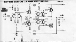
Yes, it is single ended in the first 2 stages (LTP and TR7).
What is the power supply voltage to get the 50W? Not many JFET have high Vds. And it looks like LFET is more suitable here than VFET?
For smaller power (class-A) look at Juma's F5. For similar 50W power, look at Fetzilla.
What is the power supply voltage to get the 50W? Not many JFET have high Vds. And it looks like LFET is more suitable here than VFET?
For smaller power (class-A) look at Juma's F5. For similar 50W power, look at Fetzilla.
Yes, it is single ended in the first 2 stages (LTP and TR7).
What is the power supply voltage to get the 50W? Not many JFET have high Vds. And it looks like LFET is more suitable here than VFET?
For smaller power (class-A) look at Juma's F5. For similar 50W power, look at Fetzilla.
Thanks Jay. So TR8 is not doing amplification but rather some sort of biasing or device ?
The power supply is a simple 24v AC x 2 into a bridge rectifier with large filter caps. The DC supply into the amp is approx 32v dual rails. I'm looking into building JLH 1996 dual rails after I have this amp fixed.
Tr8 is an Nchannel jFET.
It looks to me as if it's set to be a CCS load for the jFET VAS Tr7.
The 1k VR tells me that the output devices should be Lateral mosFETs.
Because the jFET Gates do not draw DC current, the currents through Tr7&8 Source resistors should be identical.
You can check the Vdrop of the 100r and 2k7 and 22k resistors around the input to find what quiescent currents are flowing.
You can also measure the offset voltages at the gates of the two input jFETs.
This then let's you add the currents flowing in the 30k resistors.
I think the output is a CFP set with gain. That gain may be 4.3 times.
Last edited:
Disclaimer: I'm not a professional - to me looks like the circuit is being unbalanced by the gate resistor (22k) to tr8 connecting to the 100 ohm input pair, causing too much current through tr8 and throwing all operating points out of kilter. What I've seen is usually connecting the resistor to the negative supply, allowing tr8 to act like a current source for tr7. But that may cause problems with not enough current to keep things balanced.
I also normally see the compensation cap (22pF) across tr7, not tr8.
Also, to me only the output stages are symmetrical - the input isn't. Just my 2 cents.
I also normally see the compensation cap (22pF) across tr7, not tr8.
Also, to me only the output stages are symmetrical - the input isn't. Just my 2 cents.
Last edited:
Thanks Andrew and Steve for your inputs. I also question the connection of the 22k. It just doesn't make sense. The 22pf on TR8 but not on TR7 raise my suspicious that the designer made a mistake. I agree the 22pf cap should be on TR7 too.
I will troubleshoot and post my findings.
- AC
I will troubleshoot and post my findings.
- AC
Good news !
Now both channels are working. I'm listening to music as I am typing this update. The channel that had a high DC offset was due to a bad cap in the NFB path, the one connects the 1000R to ground. It was leaking !!! Replaced it and measured the DC offset now at around 500mV or so. I have to correct my initial information that the original working channel also has about the same amount of DC offset. I know the DC offset is still high but at least the speaker will be able to take it for a little while.
Now for the strange part: I use a smaller transformer 18Vx2 instead of the manufacturer recommended 24Vx2 for testing. The AC output of the transformer measured equal (i.e. 18V both sides). However, the DC rails measured unequal after the bridge rectifier. The difference is 1V !!! Therefore, I think this contributes to the 500mV DC offset. I have never experience this before so I think the bridge rectifier may be bad (bad diode inside ?). Or the main filtering caps leaks ? But the caps generate no heat and they don't look "fatter" (I mean "expanded"- the problem due to heat). So I'm going to look into that and see if I can totally eliminate the DC offset problem.
Now the amp runs cold literally. I adjusted the voltage across the 1000R (trimmer) 2.7V per recommended by manufacturer for bias. I think the trimmer is to adjust quiescent current of the output FETs but without source or drain resistors at the output FET, I cannot measure the current now. I want to kick it more towards class A bias after I get it completely fixed. I think I would need a speaker protection circuit as well for the peace of mind.
The amp appears to have a very flat freq response (by listen comparison to my Musical Fidelity A1 and Tripath amp). Distortion not noticeable (but I don't have Golden ears). The sound quality definitely better than regular bipolar transistor class AB amp but seems not as good as my class A Musical Fidelity (but close). (I know people argue only the first 8W of the MF A1 is class A, but my speakers are very efficient so I listen on low settings on volume pot, but the speakers can deliver great volume into the living room).
My plan is to fix the power supply for equal rail voltages. Then adjust the 100R in the long tail pair afterwards for fine tuning of the offset. Then raise the quiescent current to kick it into class A (at least the first few watts).
Anything you guys suggest me to try as well ? What about to mod the TR8 as a CCS for 10mA (as calculated by measuring the voltage drop on TR8/TR7 source resistors ?
Thanks again ! Please feel free to comment as I am learning from this. Any more input are highly appreciated !
- AC
Update:- Stuck again.....
- Found leaking filtering caps and fixed unequal rail voltages. No changes of DC offset afterwards.
- Tried changing the values of 100Rs on LTP, DC offset swings after I paired a 1kR with one of the 100R but it settles back to the same DC offset.
- Reversed the polarity of the 220uF cap in the NFB path since it is negative at the +ve side of the cap, no change in DC offset.
I also found the DC offset voltage can swing from -300mv to -800mv at around 1Hz rate until it finally settle down to -500mv.
When I turn on the amp, I usually let it settle down for 10 seconds, then manually connects speakers. R channel is ok but L channel sometimes will trigger a very large DC offset (in less than one second) once speaker is connected (have to watch and disconnect speaker right away). But if it stables at -500mV, it will be ok and play music.
It seems to me that the amp is compensating when I change resistor values or something. I'm running out of ideas but the amp plays fine otherwise. I'm just afraid that this problem is due to FET mismatch (now both channels are having approx same DC offset and the FETs are originals with no identifiable part number).
Should I do the following ?????
1) Change TR8 to constant current sink. Set the source resistor of TR8 for 10mA (calculated from measuring voltage drop across this R and TR7's source resistor) then adjust TR7's source resistor to balance the DC offset.
2) Change the 22k at the LTP to a CCS for further stability.
3) If none of the above works, tweak drain resistors on TR6/TR4 to try to eliminate DC offset.
4) If still not working, put source or drain resistors at the output MOSFET to tune DC offset.
5) Last resort, buy matching pairs and replace them all (pray that it will work).
6) Keep the output MOSFET and build a new schematic from scratch.
Thanks in advance!
-AC
the whole front end has source resistors.
They should help stabilise the front end circuit.
The lack of source resistors in the output stage may be part of your instability problem.
I think it would be worth experimenting by adding source resistors and see if one of both versions show any improvement.
They should help stabilise the front end circuit.
The lack of source resistors in the output stage may be part of your instability problem.
I think it would be worth experimenting by adding source resistors and see if one of both versions show any improvement.
Intriguing circuit.
Initial thoughts (thinking aloud) are that this could even be supply voltage dependant. Normally a power amp (opamp configuration) works from very low voltages up to its max.
Could your supply be too low and the FET's are just not biased correctly.
The unequal supplies. If you tested with speakers connected then the DC offset will pull current from one rail or the other into the speaker and so lower one or other rail.
Thanks Andres and Mooly for ideas. I played with it a little more and I stopped when I felt (actually smelled) something's wrong.
I was about to get the output source resistors installed but I knew it will take me a while since the MOSFETs are TO-3 style and soldered directly onto the PCB with heat sink all together. While I was thinking about a way to detach them, I remember I still have that 24v x 2 transformer. Might as well see if a higher supply voltage, like Mooly said, may put them in correct bias.
I hooked up the 24v x2 tranny and power it up. The output MOSFETs are warming up (they were really running cold under 18v x 2). I checked the voltage across the VR and quickly adjusted it down to 2.7v per manual. Then I measured the DC offset (without speaker) at L channel, very low now ! But then I moved on to measure the R channel and it was higher, few volts. I felt heat rising from the driver FETs on the R channel and the drain resistor (300R, 1/2w) of TR3/4 started to turn brown. Then I stopped.........
I'm not sure if the resistors are too small (they probably are in both ohms and watts). I think after the voltage is raised, TR3/4 were having some thermal rundown. The driver FETs are small in size (like MPF102) and they are put in parallel to increase the capacity and I think it is still not enough.
So, it seems like raising supply voltage to spec fixes the DC offset. But then causing one channel unable to sustain the higher current. At this time, I am not really sure what I should do next. Since the FETs have no true part number on it, I can't really find replacement.
Any suggestions as to where I can get match N/P channels drivers jFETs ? I am really skeptical if the small FETs are able to handle this much current/voltage. Therefore, I started with a lower voltage transformer but it really caused DC offset problems. If I stay with original FETs, I probably have to tweak the resistors values a lot to fix the DC offset.
I think I'll replace that burnt resistor first and then back to the drawing board. I'm a bit confused now...............
The amp is going down the trash now. The R channel with a few volts offset has a bad 2sk19. There is a short between the gate and drain. It is fried thus causing the burning of the 300R resistor at the drain of TR5/6.
Thanks for the help but unfortunately the project ended sadly.
Thanks for the help but unfortunately the project ended sadly.
Sorry to hear that.
It sounds perhaps that although it is a circuit that could be got to work its not very repeatable given the spread of FET parameters.
It sounds perhaps that although it is a circuit that could be got to work its not very repeatable given the spread of FET parameters.
Just looking at the circuit one can conclude that there s people
that are just "designing" nightmares for other people to get on...
that are just "designing" nightmares for other people to get on...
I have more sentimental value with the amp than the its actual dollar worth. Working on this amp recalled memories that this hobby was inspired and taught by my deceased father, who was an electronic engineer and my hero "Mr. Fix-it-all". The fried power FET got me lost.....kinda of feel like you are loosing something important.....I can definitely build another amp but am gonna have a break now before back to the bench (don't know when)........
(I mistakenly referred the 2SJ18 are 2SK19 in my previous post)
(I mistakenly referred the 2SJ18 are 2SK19 in my previous post)
Whenever you feel you want a go at something else, well there are plenty of great designs on this forum and you'll get all the help you need.
If your old amp wasn't such an odd ball design I would suggest rebuilding it, but tbh there are perhaps to many unknowns with it. You would really need a variable PSU or at the very least use a "bulb tester" with it to limit current flow.
If your old amp wasn't such an odd ball design I would suggest rebuilding it, but tbh there are perhaps to many unknowns with it. You would really need a variable PSU or at the very least use a "bulb tester" with it to limit current flow.
- Status
- Not open for further replies.
- Home
- Amplifiers
- Solid State
- Need help with this schematic