I will preface this as I'm a college ECE senior trying to design a class D power amp. last semester we built a full bridge power inverter and I noticed the topology of the circuits was near identical. I'm going to build a tube pre-amp and turn this puppy in to a 50W hybrid amp for my guitar (Eventually a 100W one for Bass). But right now I want to get the power section down.
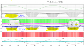
I have a question about my efficiency. You'll see from my simulated wave forms that if I look at the AVG power out / AVG power in I have an efficiency of ~98%.
Normally, I'd be super excited about this, but from experience and knowing how dumb I am, realistically the efficiency should be at around 70-80%, like with my power inverter from last semester. Also all of those spikes past a kW make me suspicious. I was wondering if there were any professional engineers on the forum that could tell me a better way on how to measure this efficiency using LtSPICE.
Any Help will be greatly appreciated.
Thanks,
Dan
Attachments

I would be sceptical about simulated efficiency as well. Be aware that you have to face hard switching at higher output levels and for my knowledge critical effects like body diode reverse recovering are not provided by the models.
At a first glance i see no protection circuitry and no overall feedback. I went the same route 2 decades ago and discovered audible nasty distortion and melting power MOSFETs. You have been warned!
At a first glance i see no protection circuitry and no overall feedback. I went the same route 2 decades ago and discovered audible nasty distortion and melting power MOSFETs. You have been warned!
For the sort of power you are dealing with 3 pairs of that particular device is overkill. One pair would do and probably something with less 'performance', higher RDSon is going to be easier to drive. Your drive IC might not like having to handle that particular burden. The 1N5817 has a VRRM of 20V and is only worth an amp. The 1N5819 has a VRRM of 40V and will be similarly stressed. Your Vbias set up for the bootstrap is questionable. You should only need the gate resistors and a bootstrap capacitor of at most 100n.
Assuming something is not breaking down and you are not suffering from cross conduction, it does not look like you should be, then the spikes are what they are and largely due to parasitic capacitances being discharged. Generally you can note their presence and ignore them.
Just some initial thoughts.
Update:
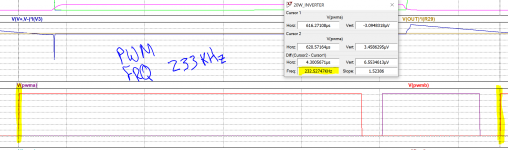
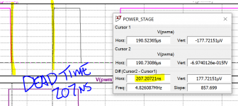
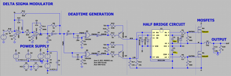
Morbid as you can see from the new circuit diagrams. I changed that bootstrap cap to 56nF and changed the bootstrap diode. This actually allowed me to run the Delta Sigma Modulator (DSM) at a higher frequency (Finally broke 300kHz). I also changed the MOSFETs to IRF540's due to your recommendation for something with a higher RDSon. The previous FETs I chose because they had a significantly lower gate charge. I also Decided to go against Dunham's Law (There's no better kill than overkill,) and go with your advice to remove all of the extra FETs and simplify down the network between the driver and FETs.
Bucks I did try and add some feedback from the output to the negative end of a buffer amp going in to the DSM but after about 3 hours of sitting at 100pS, I decided to try it out later this week when start to build a perfboard prototype later this week. As far as protection circuity what would you recommend I'm in more so of the computer end of the ECE program at school and they don't really go into this to much for us I've tried looking it up on google and kind of get confused about what I'm looking at. I was actually wondering if what you mean is some sort of current limiting circuity to try and reduce all of those current spikes. Or did you mean some sort of a soft start circuity.
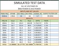
Also to any one else I have some included data gathered from simulations across the range of human hearing.
Again thanks for the help,
Dan.
Morbid as you can see from the new circuit diagrams. I changed that bootstrap cap to 56nF and changed the bootstrap diode. This actually allowed me to run the Delta Sigma Modulator (DSM) at a higher frequency (Finally broke 300kHz). I also changed the MOSFETs to IRF540's due to your recommendation for something with a higher RDSon. The previous FETs I chose because they had a significantly lower gate charge. I also Decided to go against Dunham's Law (There's no better kill than overkill,) and go with your advice to remove all of the extra FETs and simplify down the network between the driver and FETs.
Bucks I did try and add some feedback from the output to the negative end of a buffer amp going in to the DSM but after about 3 hours of sitting at 100pS, I decided to try it out later this week when start to build a perfboard prototype later this week. As far as protection circuity what would you recommend I'm in more so of the computer end of the ECE program at school and they don't really go into this to much for us I've tried looking it up on google and kind of get confused about what I'm looking at. I was actually wondering if what you mean is some sort of current limiting circuity to try and reduce all of those current spikes. Or did you mean some sort of a soft start circuity.
Also to any one else I have some included data gathered from simulations across the range of human hearing.
Again thanks for the help,
Dan.
Attachments

I cannot provide any convincing protection circuitry and this was the main reason I gave up building discrete class-d-amps more than 20yrs ago. If you are looking for high-power solutions with hundreds of Watts the IRS-drivers (now Infineon) seem to be a reliable solution. Personnaly I operate inside the 100W region - where TI-chips like TPA3255 are my choice. All these nasty problems I never addressed are solved with these chips, so why re-invent the wheel?😉