I'm very new to solid state designs, and I'm attempting to design a high voltage amplifier to drive the grids of output tubes.
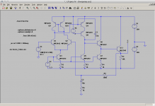
I whipped this up (see attachment) in LTSpice and it works, suspiciously well in fact, I'm getting readings of 0.009% distortion at 20Khz while swinging 100V P-P into the 10k load resistor, with the gain set to 100 (well, near enough)
Now, I'm not 100% trustworthy of this result, seeing as it seems pretty good, and I basically happened upon this design by accident / fiddling. For example, I'm not sure if my current mirror is actually doing anything useful, as it's driving the low impedance input of the VAS transistor.
Basically it would be really great if someone could look over this design for me and suggest improvements where possible 😀
Thanks for any help 😀
Attachments
What tube are you driving?
I don't know yet - most likely pentode mode EL34s or KT88s, I'm just trying to develop a circuit that can easily drive pretty much anything. It is probably overkill but it's an interesting excercise in itself
Member
Joined 2009
Paid Member
what is the advantage in this approach, over say, an all-tube design ? - is it simply that you have lower distortion given all the nfb ?
It would be interesting to hear this circuit, if the distortion is really low it would allow the harmonic signature of the output tube to come through.
It would be interesting to hear this circuit, if the distortion is really low it would allow the harmonic signature of the output tube to come through.
Don't forget that any circuit which relies on transistor balance (e.g. LTP, current mirror) will always simulate with lower distortion than in real life.
what is the advantage in this approach, over say, an all-tube design ? - is it simply that you have lower distortion given all the nfb
Convenience mainly - it would be cool to have a simple universal circuit you can make up on a small PCB and have it drive nearly any valve!
Does anyone have any comment on the circuit itself? Am I doing anything stupid? Are there faster / better transistors I could use?
Does anyone have any comment on the circuit itself?
One could probably write a book on it--but you're not saying what your goals are. Distortion? Noise? Cost/complexity? Quiescent current? Bandwidth?
As a starter: a current mirror usually benefits greatly from emitter degeneration, e.g. to reduce noise and sensitivity to transistor mismatch.
Samuel
One could probably write a book on it--but you're not saying what your goals are. Distortion? Noise? Cost/complexity? Quiescent current? Bandwidth?
As a starter: a current mirror usually benefits greatly from emitter degeneration, e.g. to reduce noise and sensitivity to transistor mismatch.
Samuel
My goals would be wide bandwidth / high slew rate and low distortion - I like to fiddle with valve circuits it would be cool to build these as little gain modules you can really "lean" on and know they will perform well.
I added 100 ohm resistors to the current mirror and it increased the overall open loop gain somewhat and of course would have the positive effect you described of being less critical about transistor mismatch
forgive my ignorance but what are the parts that look like filter caps marked a V1 through V6 ? Are these d.c. batteries you are using in an active circuit ?
Tubes are voltage amplifiers ( rather "charge change amplifiers) and BJTs are current amplifiers. The respective physics of amplification are entirely different.
It makes no sense to drive a voltage amp with a current amp you could easily replace the BJT high V with one or two tubes and stay so to speak in one family of amplification.
It makes no sense to drive a voltage amp with a current amp you could easily replace the BJT high V with one or two tubes and stay so to speak in one family of amplification.
I've got a couple of thoughts. Look at the current (and thus the power!) in each transistor - with about 100V across each one, it doesn't take much current to exceed their power rating. R2 at 10k and 100V has 10mA going through it, so it dissipates 1 watt, and so does Q6. I just looked up the part number, and see it's big enough to do that.
The current sources look like 700uA, or 70mW in the transistors with 100V on them.
I wasn't sure you need Q6, Q7 and Q11, but then for an output tube I can see where you may want to drive a grid positive where it will pull significant grid current.
So yes, it looks good to me.
The current sources look like 700uA, or 70mW in the transistors with 100V on them.
I wasn't sure you need Q6, Q7 and Q11, but then for an output tube I can see where you may want to drive a grid positive where it will pull significant grid current.
So yes, it looks good to me.
Those are ideal voltage sources in the simulator. V1 and V2 are the DC +/-100V power supply, V3 is the input signal used to test distortion and frequency response, and the other two will be presumably be replaced by series resistor and diode chains to bias the current sources and mirrors.forgive my ignorance but what are the parts that look like filter caps marked a V1 through V6 ? Are these d.c. batteries you are using in an active circuit ?
- Status
- Not open for further replies.
- Home
- Amplifiers
- Solid State
- My HV opamp - Working suspiciously well