Hi. I'm building this intringuing TDA-1541 DAC with a friend, the AYA-DAC ver 2.0c, see: http://www.pedjarogic.com/1541a/rev2.htm
However this particular design need as a supply a custom transformer with more than 8 separates AC secondaries.
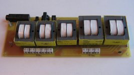
I design a custom PCB that accept 5 separates transformers and can supply all the AC suppllies needed by the AYA-DAC. The transformers are not expensive, about 6U$ each for the three 8Vac transfos and 8U$ each for the two 18Vac transfos. They are easily available from Digikey. This alternative will give the same supply insulation as a custom transformer but at a much cheaper price. The choosen transformers are split bobbins type that has low coil couplings providing an excellent insulation without using a static shield as needed when using a toroidal transfo. This is the type of transformer recommend for preamp use by John Curl himself as discussed on the Blowtorch thread
The PCB will have these features:
-Pads available for AC input and fuse socket
-Provision for an input C-L-C EMI AC input filter
-Dual Primaries transfo and easy solder jumper Main Ac voltage selection (120-240, 110-220V)
-Provision for an Main Power-On Switch
-Built in Power-On Led circuit and header 2-pins socket
-AC Output on the same screw terminal as used on the AYA Dac.
I'm planning to build and test a prototype in the next few weeks.
Pass the word on Yahoo.
I'm building my own PCB. I may build some more if some other users are interested.
However this particular design need as a supply a custom transformer with more than 8 separates AC secondaries.
I design a custom PCB that accept 5 separates transformers and can supply all the AC suppllies needed by the AYA-DAC. The transformers are not expensive, about 6U$ each for the three 8Vac transfos and 8U$ each for the two 18Vac transfos. They are easily available from Digikey. This alternative will give the same supply insulation as a custom transformer but at a much cheaper price. The choosen transformers are split bobbins type that has low coil couplings providing an excellent insulation without using a static shield as needed when using a toroidal transfo. This is the type of transformer recommend for preamp use by John Curl himself as discussed on the Blowtorch thread
The PCB will have these features:
-Pads available for AC input and fuse socket
-Provision for an input C-L-C EMI AC input filter
-Dual Primaries transfo and easy solder jumper Main Ac voltage selection (120-240, 110-220V)
-Provision for an Main Power-On Switch
-Built in Power-On Led circuit and header 2-pins socket
-AC Output on the same screw terminal as used on the AYA Dac.
I'm planning to build and test a prototype in the next few weeks.
Pass the word on Yahoo.
I'm building my own PCB. I may build some more if some other users are interested.
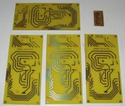
Take note that I had two pre-requisites when designing the PCB. It has to fit into a nice case that I already had in stock. This explain some of the strange mounting hole locations. It also had to fit into the maximum PCB sheet material that I'm using. Here the first version of this PCB.
Attachments
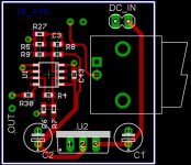
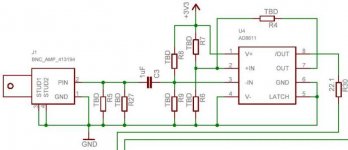
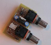
I'm also designing an active BNC digital input PCB, based on the same AD8611 High-Speed 4ns comparator used into the Headphone DAC project. This version version is using a local 3.3V regulator supplies from the DAC 5V supply. This is probably not the final version of this PCB. I want to add a relay to switch between to inputs, this active one and the original AYA DAC transfo coupled. By using a front mounted switch it will be possible to switch between these two inputs.
There is also provision to use this bare PCB only as a mounting PCB for the true 75 ohms BNC, 31-10-75 Amphenol connector that I will use.
Since both inputs are using a different approach, active and transfo coupled, it will be possible to choose the one with the best sound for your application.
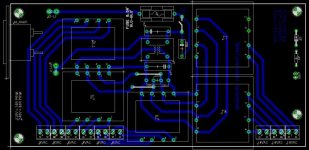
Here my first pcb version. The bottom layer is the gnd plane.
There is also provision to use this bare PCB only as a mounting PCB for the true 75 ohms BNC, 31-10-75 Amphenol connector that I will use.
Since both inputs are using a different approach, active and transfo coupled, it will be possible to choose the one with the best sound for your application.
Here my first pcb version. The bottom layer is the gnd plane.
Attachments
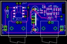
Here the input PCB ver 1.2 that support 2 inputs, one active before the transfo, the other directly to the transfo as the original design. A small SMD Omron relay selects what input. The direct connection is selected by default. Just add a switch and you can easily select the input.
Attachments
I am interested in your transformer PCB. I am building the same dac and purchased two large transformers, but they are more difficult to fit into a chassis. Let me know if you are interested in selling a PCB.
Yes, no problem. I can make a small run of these PCB. They are excellent quality FR4 PCB. You can solder plate the traces yourself or I can do it for you for a small fee. It will be all drilled ready to use. I'll do a small change to it to use a more common fuse holder. I can do it in the next weeks. Send me an email.
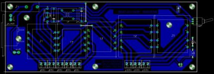
Following Pedja Rogic advice, I did a ver 2.0 of the transfo PCB with minimum spacing of 4mm for the HV traces as recommended into the safety regulation. The PCB is also smaller. I also added the 6th 8Vac output as it can be use into an upcoming AYA version as Pedja suggested. I think it is a better design. Thanks for the tips 😉
See the included image. Take note I still have a few traces to do to complete the pcb. Should be done by tomorrow.
That will be the version that I will build for a few guys.
Bye...
SB
See the included image. Take note I still have a few traces to do to complete the pcb. Should be done by tomorrow.
That will be the version that I will build for a few guys.
Bye...
SB
Attachments
Transfo PCB ver 2.0 is completed. I'll make a small change to the transfo parts list. For the 16Vac transfo I'll use a lower sec. voltage than the one originally specified. The 16Vac supplies are sinking about 120-150ma maximum, so the 1A/16Vac specified originally for the DAC are causing that the transfo is working almost on no load, so the secondary voltage is much higher. Futhermore the one I choose was for 110V/220V and was specs to give 18Vac at full load with is not the case at all in the AYA DAC. So the MT2124-ND, 18Vac secondary, 0.7A gives about 23.8Vac connected to the DAC (with 120Vac and the transfo regulation), way too high and causing overheat of the shunt regulator. The MT2120-ND, 14Vac, 0.8A will give about 18.6Vac in the same condition, almost on mark with the 18Vac maximum recommended. It will give about 17V is used with 110/220Vac. So this is the correct part to use.
You probably means that the 16V and 8V outputs are not perfectly aligned with the AYA DAC PCB own input connectors.
It was almost impossible to make this happen and keep the transfo PCB not too big. If you look at the AYA DAC the 16V ac are mixed with the 8Vinputs.
One requirement for the transfo PCB, since I'm routing high voltages 120/240V, was to space the PCB traces with a minimum of 4mm everywhere! That mean a lot of PCB real estate spent just for insulation between traces.
I also tried to reduced to a minimum High voltage and low voltage traces lenght. Then to reduce cross transfo induction, the 16V transfo are mounted 90deg from the 8V transfo, mixing traces even more. Finally I also wanted to keep this PCB single side to keep all traces under the board for safety. All in all, these requirements prevented me from aligning perfectly the DAC and transfo PCB connector and keep the transfo PCB to a reasonnable size.
Never forget that we route AC voltages from the transfo PCB to the DAC. To do so it is better to use twisted wire pairs for each voltage. So we need some space between each PCB to route these twisted pairs. It is not like the transfo PCB was a DC low voltage power supply pcb, requirements were different from the start. Anyway, the connectors are almost aligned, so the lenght of twisted wires will be rather short. Don't forget that AC current will be lower than DC, so a small lenght of twisted wire won't have any real impact on supply power delivery.
Finally don't forget either that an actual custom transformer would have a lot of outputs wires that you would need to route also to the correct input conenctors.
I kind of like to think about this transfo pcb as an actual transformer, not a power supply pcb.
This is not a commercial venture here, just my own solution that I proposed to other to maybe solve the same problem that I had with the expensive custom power transformer. It is a much cheaper and easier solution. Pedja himself find it usefull.
Bye...
SB
No problem. In fact Pedja help me to get the PCB more safe and gave me quite a few usefull comments about it. Thanks Pedja.
I tested the full transfo PCB ver 2.0 with the actual AYA DAC load and refined my choice of transfo. It is working perfectly with almost exact 8 and 16Vac outputs under load.
- Status
- Not open for further replies.
- Home
- Source & Line
- Digital Source
- My AYA-DAC ver 2.0c Accessories PCB's