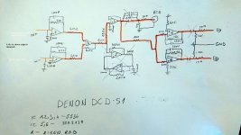
I have reverse engineered DCD-S-1 IV output stage (4x pcm1702) as no schematics were possible to acquire. it have really nice passive parts but seems some strange desisions like diferent ground resistors for balanced out(6.7K and 20K- triple checked that), and high output resistors(4.23K, 6.7K)
IC5 GIC filter (?) seems also best ommited.
If understand corectly schematics IC 1,2 is I to V converters, IC4, summing amp, IC 3 bufer, IC6 SE to diferential with gain less than 1?
I would like to have dedicated balanced out(5-6V RMS) instead of suming and balancing again (RCA- 3V rms)
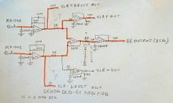
my preliminary modified schematics is here, I have reduced most resistors to 2K as I have plenty of them (Vishay metal bulk foils) I ahve also included direct out for xlr as sugested. Enclosure is big I can make extra few holes foraditional XLR. (I supose direct XLR out wont be sucifient for 10K input impedance ampas with gain less than 28db)
opinions and corections needed. thanks in advance.
IC5 GIC filter (?) seems also best ommited.
If understand corectly schematics IC 1,2 is I to V converters, IC4, summing amp, IC 3 bufer, IC6 SE to diferential with gain less than 1?
I would like to have dedicated balanced out(5-6V RMS) instead of suming and balancing again (RCA- 3V rms)
my preliminary modified schematics is here, I have reduced most resistors to 2K as I have plenty of them (Vishay metal bulk foils) I ahve also included direct out for xlr as sugested. Enclosure is big I can make extra few holes foraditional XLR. (I supose direct XLR out wont be sucifient for 10K input impedance ampas with gain less than 28db)
opinions and corections needed. thanks in advance.
Attachments
Last edited:
IC1 and IC2 voltage follower with lead compensation.
IC4 differential amp.
IC3 voltage follower.
IC5 dc servo?
IC6 is rubbish single ended to differential output.
The 2k ohm input resistor for IC 4 (modified) is incorrect, please verify again.
If I were you, just use the output for IC1 and IC2 for balance out is sufficient.
Here's a datasheet for your reference.
http://ohm.bu.edu/~pbohn/STM-Z-BERKELEY/Data_Sheets/stm_zbox/PCB/PCM1702.pdf
Hi Jason, thanks for quick reply. input is CURRENT, not voltage (my schematcis is incomplete- ommiting pcm1702 current output leg, sorry ddnt thought about it while drawing ,my fault)
non inverting IC4 (modified) 2K input resistor with 2.65K feedback resistor sets gain to x2.3 if i leave 4.2k/2.65K I get x1.4 gain. I would like to get 3V RMS output instead of 2V RMS. my RC filters(2K/2700pf) is also a bit low (comparing to original 1.27K/2700pf)
non inverting IC4 (modified) 2K input resistor with 2.65K feedback resistor sets gain to x2.3 if i leave 4.2k/2.65K I get x1.4 gain. I would like to get 3V RMS output instead of 2V RMS. my RC filters(2K/2700pf) is also a bit low (comparing to original 1.27K/2700pf)

IC5 kinda looks like an active filter, maybe gyrator. Have to think about it some more.
EDIT: If a current out dac with opamp I/V then IC1,2 are probably for that. In that case the dac outputs would need to go to the inverting inputs. A reference voltage may go the the noninverting inputs.
EDIT: If a current out dac with opamp I/V then IC1,2 are probably for that. In that case the dac outputs would need to go to the inverting inputs. A reference voltage may go the the noninverting inputs.
Last edited:
I think ic5 (2139 opamp) is GIC filter. I plan to remoove it. Inversion on phase is done digitaly in lamba processor ( which are after two alpha processors and sm5843) so output from pcm1702 leg is balanced already. Basicaly I want confirmation from more expierenced diyers that my mod of ading separate balance output is ok with values i choose to get 5-6V RMS XLR and 2.5-3 single ended. I kept all inverting non inverting op amps as it were stock.
good point , of course I out goes to inverting pin, just when redraw schematics I accidently placed wrong input path mark. corrected and added new direct XLR out.EDIT: If a current out dac with opamp I/V then IC1,2 are probably for that. In that case the dac outputs would need to go to the inverting inputs.
Last edited:
I have reverse engineered DCD-S-1 IV output stage (4x pcm1702) as no schematics were possible to acquire. it have really nice passive parts but seems some strange desisions like diferent ground resistors for balanced out(6.7K and 20K- triple checked that), and high output resistors(4.23K, 6.7K)
IC5 GIC filter (?) seems also best ommited.
If understand corectly schematics IC 1,2 is I to V converters, IC4, summing amp, IC 3 bufer, IC6 SE to diferential with gain less than 1?
I would like to have dedicated balanced out(5-6V RMS) instead of suming and balancing again (RCA- 3V rms)
my preliminary modified schematics is here, I have reduced most resistors to 2K as I have plenty of them (Vishay metal bulk foils) I ahve also included direct out for xlr as sugested. Enclosure is big I can make extra few holes foraditional XLR. (I supose direct XLR out wont be sucifient for 10K input impedance ampas with gain less than 28db)
opinions and corections needed. thanks in advance.
- Home
- Source & Line
- Digital Line Level
- Modifying Denon DCD-S1 IV stage,opinions needed